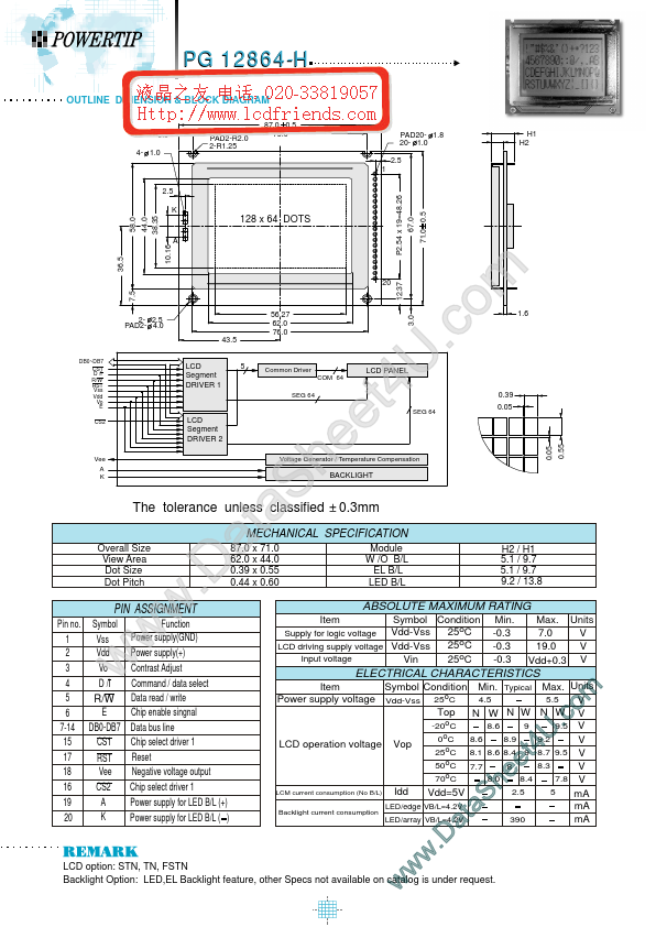
PG 12864-H
OUTLINE DIMENSION & BLOCK DIAGRAM
87.0 0.5 75.0
6.0 4- 1.0
PAD2-R2.0 2-R1.25
PAD20- 1.8 20- 1.0 2.5 1
H1 ...
PG 12864-H
OUTLINE DIMENSION & BLOCK DIAGRAM
87.0 0.5 75.0
6.0 4- 1.0
PAD2-R2.0 2-R1.25
PAD20- 1.8 20- 1.0 2.5 1
H1 H2
2.5 71.0 0.5 K 44.0 38.35 58.0 P2.54 x 19=48.26 67.0
128 x 64 DOTS
10.16 A
36.5
7.5
12.37
20
2- 2.5 PAD2- 4.0 43.5
DB0~DB7 CS1 D /I R/W RST Vss Vdd Vo E CS2
56.27 62.0 76.0
LCD Segment DRIVER 1
5
Common Driver COM 64 SEG 64
LCD Segment DRIVER 2
Vee A K
The tolerance unless classified
Overall Size View Area Dot Size Dot Pitch
PIN ASSIGNMENT
Pin no. 1 2 3 4 5 6 7-14 15 17 18 16 19 20 Symbol Vss Vdd Vo D /I R/W E DB0-DB7 CS1 RST Vee CS2 A K
w
Function Power supply(GND) Power supply(+) Contrast Adjust Command / data select Data read / write Chip enable singnal Data bus line Chip select driver 1 Reset Negative
voltage output Chip select driver 1
w
w
.D
87.0 x 71.0 62.0 x 44.0 0.39 x 0.55 0.44 x 0.60
t a
MECHANICAL SPECIFICATION
Module W /O B/L EL B/L LED B/L H2 / H1 5.1 / 9.7 5.1 / 9.7 9.2 / 13.8
S a
Voltage Generator / Temperature Compensation
e h
Item
BACKLIGHT
0.3mm
ABSOLUTE MAXIMUM RATING
Symbol Condition Vdd-Vss 25oC 25oC LCD driving supply
voltage Vdd-Vss Input
voltage 25oC Vin
Supply for logic
voltage
Min. -0.3 -0.3 -0.3
Max. Units V 7.0 19.0 V Vdd+0.3 V Max. Units 5.5 V N W V 9.5 V
ELECTRICAL CHARACTERISTICS
Item Power supply
voltage Symbol Condition
Vdd-Vss 25oC
0.05
Min. Typical
4.5
Top
-20oC 0oC
N W N W
8.6 8.6 8.9 9
Power supply for LED B/L (+) Power supply for LED B/L ( )
V V 50oC 8.3 7.7 8 V 7.8 V 8.0 8.4 70o...