www.DataSheet4U.com
xr
FEBRUARY 2006
PRELIMINARY
XRK39351
REV. P1.0.0
3.3V OR 2.5V, 9-OUTPUT PLL CLOCK DRIVER
input ...
www.DataSheet4U.com
xr
FEBRUARY 2006
PRELIMINARY
XRK39351
REV. P1.0.0
3.3V OR 2.5V, 9-OUTPUT PLL CLOCK DRIVER
input is pulled low. This is a test mode intended for system debug purposes. The XRK39351 has an output/input frequency range of 25MHz to 200MHz with the PLL enabled and an input frequency range of 2MHz to 300MHz when the PLL is disabled (test mode). FEATURES
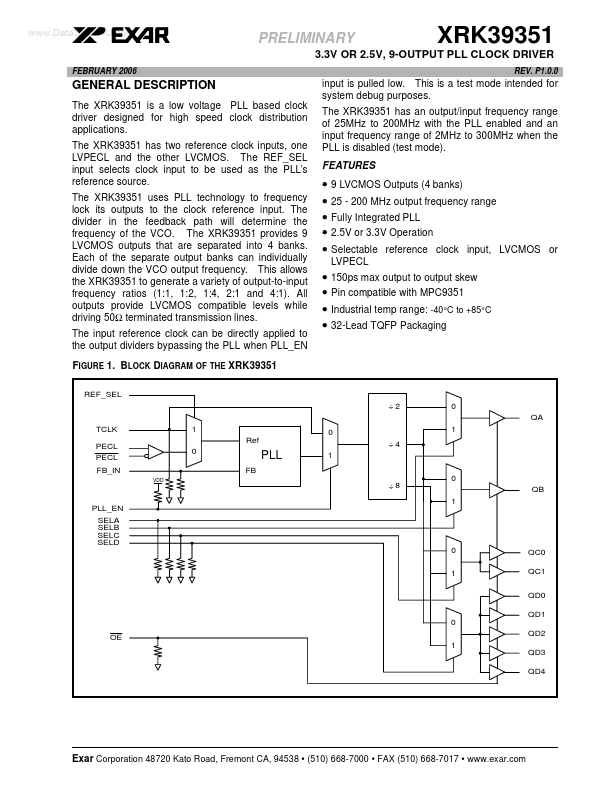
GENERAL DESCRIPTION
The XRK39351 is a low
voltage PLL based clock driver designed for high speed clock distribution applications. The XRK39351 has two reference clock inputs, one LVPECL and the other LV
CMOS. The REF_SEL input selects clock input to be used as the PLL’s reference source. The XRK39351 uses PLL technology to frequency lock its outputs to the clock reference input. The divider in the feedback path will determine the frequency of the VCO. The XRK39351 provides 9 LV
CMOS outputs that are separated into 4 banks. Each of the separate output banks can individually divide down the VCO output frequency. This allows the XRK39351 to generate a variety of output-to-input frequency ratios (1:1, 1:2, 1:4, 2:1 and 4:1). All outputs provide LV
CMOS compatible levels while driving 50Ω terminated transmission lines. The input reference clock can be directly applied to the output dividers bypassing the PLL when PLL_EN FIGURE 1. BLOCK DIAGRAM OF THE XRK39351
REF_SEL
9 LV
CMOS Outputs (4 banks) 25 - 200 MHz output frequency range Fully Integrated PLL 2.5V or 3.3V Operation Selectable reference clo...