WTC2309
P-Channel Enhancement Mode Power MOSFET
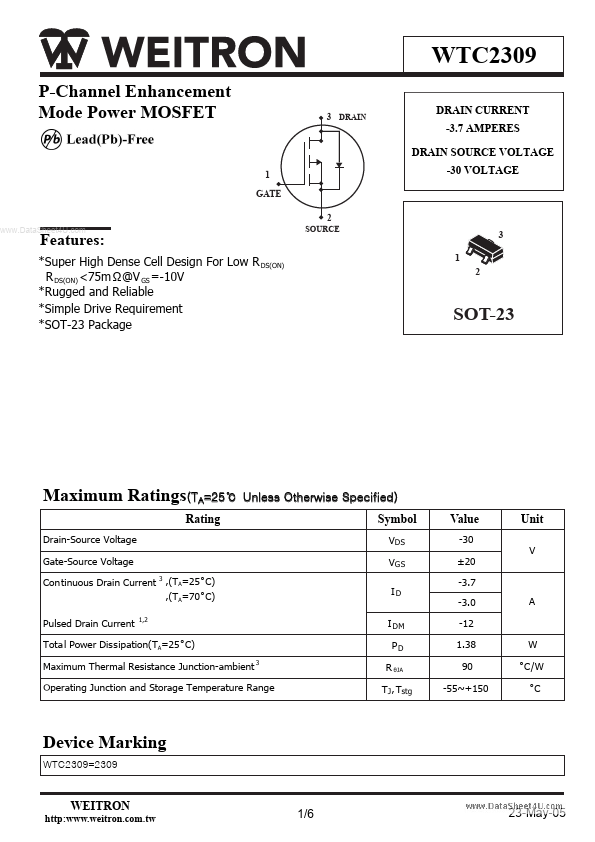
1 GATE
SOURCE
3 DRAIN
DRAIN CURRENT -3.7 AMPERES DRAIN SOURCE VOLTAGE ...
WTC2309
P-Channel Enhancement Mode Power
MOSFET
1 GATE
SOURCE
3 DRAIN
DRAIN CURRENT -3.7 AMPERES DRAIN SOURCE
VOLTAGE -30
VOLTAGE
2
www.DataSheet4U.com
Features:
3 1 2
*Super High Dense Cell Design For Low R DS(ON) R DS(ON) <75m Ω@V GS =-10V *Rugged and Reliable *Simple Drive Requirement *SOT-23 Package
SOT-23
Maximum Ratings(TA=25℃
Rating
Drain-Source
Voltage Gate-Source
Voltage Continuous Drain Current 3 ,(TA=25˚C) ,(TA=70˚C) Pulsed Drain Current
1,2
Unless Otherwise Specified) Symbol
VDS VGS ID I DM PD R θJA TJ , Tstg
Value
-30 ±20 -3.7 -3.0 -12 1.38 90 -55~+150
Unit
V
A
Total Power Dissipation(TA=25˚C) Maximum Thermal Resistance Junction-ambient 3 Operating Junction and Storage Temperature Range
W ˚C/W ˚C
Device Marking
WTC2309=2309
http:www.weitron.com.tw
WEITRON
1/6
23-May-05
WTC2309
Electrical Characteristics (TA = 25℃
Characteristic Unless otherwise noted) Symbol Min Typ Max Unit
Static
Drain-Source Breakdown
Voltage VGS =0,I D =-250μA www.DataSheet4U.com Gate-Source Threshold
Voltage VDS =VGS ,I D =-250 μA Gate-Source Leakage Current VGS = ±20V Drain- Sou rce Leakage Current(Tj=25˚C) VDS =-30V,V GS =0 Drain- Sou rce Leakage Current(Tj=55˚C) VDS =-24V,V GS =0 Drain-Source On-Resistance 2 VGS =-10V,I D=-3.0A VGS =-4.5V,I D=-2.6A Forward Transconductance VDS =-10V, ID =-3A g fs R DS(o n) 5.0 75 120 mΩ I DSS -25 V(BR)DSS VGS(Th) I GSS -30 -1.0 V -3.0 ±100 -1 μA nA
S
Dynamic
Input Capacitance VGS =0V,VDS =-25V,f=1.0MHz Output Capacitance VGS =0V,VD...