WTC2304
N-Channel Enhancement Mode Power MOSFET
P b Lead(Pb)-Free
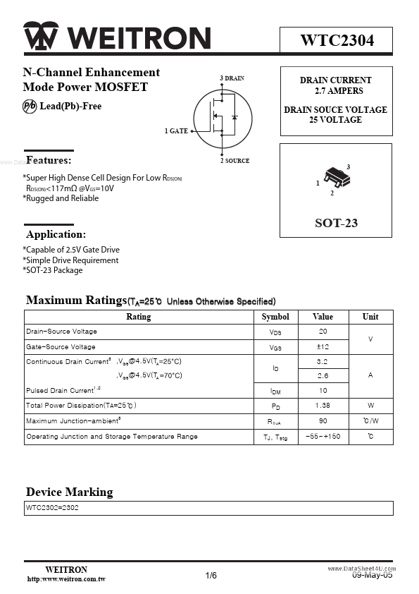
1 GATE 3 DRAIN
DRAIN CURRENT 2.7 AMPERS DRAIN SOUCE V...
WTC2304
N-Channel Enhancement Mode Power
MOSFET
P b Lead(Pb)-Free
1 GATE 3 DRAIN
DRAIN CURRENT 2.7 AMPERS DRAIN SOUCE
VOLTAGE 25
VOLTAGE
www.DataSheet4U.com
Features:
2 SOURCE
3 1 2
*Super High Dense Cell Design For Low RDS(ON) RDS(ON)<117mΩ @VGS=10V *Rugged and Reliable
Application:
*Capable of 2.5V Gate Drive *Simple Drive Requirement *SOT-23 Package
SOT-23
Maximum Ratings(TA=25℃
Rating
Drain-Source
Voltage Gate-Source
Voltage Continuous Drain Current3 ,
[email protected](TA ,
[email protected](TA Pulsed Drain Current1,2 Total Power Dissipation(TA=25 ℃ ) Maximum Junction-ambient3
Unless Otherwise Specified) Symbol
VDS VGS ID IDM PD R
JA
Value
20 ±12 3.2 2.6 10 1.38 90 -55~+150
Unit
V
A
W ℃/W ℃
Operating Junction and Storage Temperature Range
TJ, Tstg
Device Marking
WTC2302=2302
http:www.weitron.com.tw
WEITRON
1/6
09-May-05
WTC2302
Electrical Characteristics (TA = 25℃
Characteristic Unless otherwise noted) Symbol Min Typ Max Unit
Static
Drain-Source Breakdown
Voltage VGS=0,ID=250μA www.DataSheet4U.com Gate-Source Threshold
Voltage VDS=VGS,ID=250μA Gate-Source Leakage Current VGS= ±12V Drain-Source Leakage Current(Tj=25℃) VDS=20V,VGS=0 Drain-Source Leakage Current(Tj=70℃) VDS=20V,VGS=0 Drain-Source On-Resistance VGS=4.5V,ID=3.6A VGS=2.5V,ID=3.1A Forward Transconductance VDS=5V,ID=3.6A gfs RDS(on) 6 85 115 mΩ IDSS 10 V(BR)DSS VGS(Th) IGSS 20 0.5 V 1.2 ±100 1 μA nA
S
Dynamic
Input Capacitance VGS=0V,VDS=10V,f=1.0MHz Output Capacitance VGS=0V,VDS=10V,f=1.0MHz Reverse Transf...