SDRAM UNBUFFERED
White Electronic Designs
W3DG72128V-D2
PRELIMINARY*
1GB- 128Mx72 SDRAM, REGISTER and SPD, w/PLL
FEATURES
Clock speed o...
Description
White Electronic Designs
W3DG72128V-D2
PRELIMINARY*
1GB- 128Mx72 SDRAM, REGISTER and SPD, w/PLL
FEATURES
Clock speed of 100MHz and 133MHz Burst Mode Operation Auto and Self Refresh capability LVTTL compatible inputs and outputs Serial Presence Detect with EEPROM Fully synchronous: All signals are registered on the positive edge of the system clock Programmable Burst Lengths: 1, 2, 4, 8 or Full Page 3.3V ± 0.3V Power Supply 168 Pin DIMM JEDEC
* This product is under development, is not qualified or characterized and is subject to change without notice.
DESCRIPTION
The W3DG72128V is a 128Mx72 synchronous DRAM module which consists of eighteen 128Mx4 stack SDRAM components in TSOP II package, two 18 bit Drive ICs for input control signal and one 2Kb EEPROM in an 8 pin TSSOP package for Serial Presence Detect which are mounted on a 168 pin DIMM multilayer FR4 Substrate.
www.DataSheet4U.com
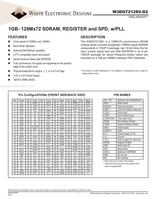
Pin ConfigurATIONs (FRONT SIDE/BACK SIDE)
Pin 1 2 3 4 5 6 7 8 9 10 11 12 13 14 15 16 17 18 19 20 21 22 23 24 25 26 27 28 Front VSS DQ0 DQ1 DQ2 DQ3 VCC DQ4 DQ5 DQ6 DQ7 DQ8 VSS DQ9 DQ10 DQ11 DQ12 DQ13 VCC DQ14 DQ15 CB0 CB1 VSS NC NC VCC WE# DQM0 Pin 29 30 31 32 33 34 35 36 37 38 39 40 41 42 43 44 45 46 47 48 49 50 51 52 53 54 55 56 Front DQM1 CS0# DNU VSS A0 A2 A4 A6 A8 A10/AP BA1 VCC VCC CLK0 VSS DNU CS2# DQM2 DQM3 DNU VCC NC NC CB2 CB3 VSS DQ16 DQ17 Pin 57 58 59 60 61 62 63 64 65 66 67 68 69 70 71 72 73 74 75 76 77 78 79 80 81 82 83 84 Front DQ18 DQ19 VCC DQ20 NC *VREF *CKE1 VSS DQ21 DQ22 DQ2...
Similar Datasheet