Preliminary W27C4096 256K × 16 ELECTRICALLY ERASABLE EPROM
GENERAL DESCRIPTION
The W27C4096 is a high speed, low power E...
Preliminary W27C4096 256K × 16 ELECTRICALLY ERASABLE EPROM
GENERAL DESCRIPTION
The W27C4096 is a high speed, low power Electrically Erasable and Programmable Read Only Memory organized as 262144 × 16 bits that operates on a single 5 volt power supply. The W27C4096 provides an electrical chip erase function.
FEATURES
High speed access time:
120/150 nS (max.) Read operating current: 30 mA (max.) Erase/Programming operating current 30 mA (max.) Standby current: 100 µA (max.) Single 5V power supply
+14V erase/+12V programming
voltage Fully static operation All inputs and outputs directly TTL/
CMOS
compatible
Three-state outputs Available packages: 40-pin 600 mil DIP, TSOP
and 44-pin PLCC
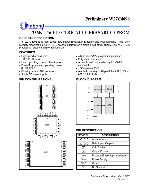
PIN CONFIGURATIONS
VPP CE Q15 Q14 Q13 Q12 Q11 Q10 Q9 Q8 GND Q7 Q6 Q5 Q4 Q3 Q2 Q1 Q0 OE
1 2 3 4 5 6 7 8 9 10 11 12 13 14 15 16 17 18 19 20 40 39 38 37 36 35 34 33 32 31 30 29 28 27 26 25 24 23 22 21
BLOCK DIAGRAM
VDD A17 A16 A15 A14 A13 A12 A11 A10 A9 GND A8 A7 A6 A5 A4 A3 A2 A1 A0
Q0 CE OE CONTROL OUTPUT BUFFER
. .
Q15
40-pin DIP
A0
. .
A17
DECODER
CORE ARRAY
Q 1 3 6 Q12 Q11 Q10 Q9 Q8 GND NC Q7 Q6 Q5 Q4 7 8 9 10 11 12 13 14 15 16 17 18 Q 3
Q 1 4 5
Q 1 5 4
/ C E
V p p 2
N C 1
V
C C
A 1 7
A 1 6 42
A 1 5 41
A 1 4 40 39 38 37 36 A13 A12 A11 A10 A9 GND NC A8 A7 A6 A5
VCC GND VPP
3
44 43
44-pin PLCC
35 34 33 32 31 30 29
PIN DESCRIPTION
SYMBOL A0−A17
40 39 38 37 36 35 34
19 Q 2
20 21 Q 1
22
23 24 25 N C A 0
26 27 A 2 A 3
28
Q 0
/ O E
A 1
A 4
D...