www.DataSheet4U.com
DATA SHEET
MOS INTEGRATED CIRCUIT
μ PD121A10
2-POWER SUPPLY INPUT METHOD 1.0 V/2.0 A REGULATOR
D...
www.DataSheet4U.com
DATA SHEET
MOS INTEGRATED CIRCUIT
μ PD121A10
2-POWER SUPPLY INPUT METHOD 1.0 V/2.0 A REGULATOR
DESCRIPTION
μ PD121A10 is the
CMOS regulator which can output 2.0 A current. This regulator is suitable for power supply for 1.0 V ASIC core, for example our companies’ CB-90 (90 nm process LSI) etc. The dropout
voltage is made small (0.7 V MAX. (IO = 1.0 A) by dividing bias
voltage (VDD) from input
voltage (VIN). Therefore this product can output under the conditions, VIN ≥ 1.62 V (VDD ≥ 4.0 V). Output
voltage can be adjustable between 0.95 and 1.15 V.
FEATURES
Output Current: 2.0 A Output
Voltage: 0.95 to 1.15 V Bias
Voltage: 4.0 to 5.5 V Reference
Voltage Tolerance: VREF ± 10 mV (TJ = 25°C) Low Dropout
Voltage: VDIF = 0.7 V MAX. (IO = 1.0 A) On-chip over-current protection circuit On-chip thermal shut down circuit
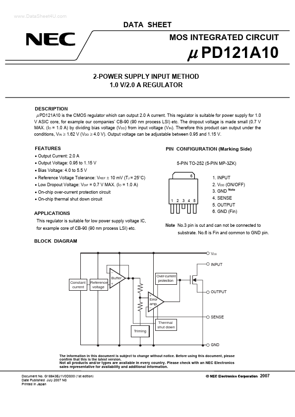
PIN CONFIGURATION (Marking Side)
5-PIN TO-252 (5-PIN MP-3ZK)
6
1. INPUT 2. VDD (ON/OFF) 3. GND
Note
1 2 3 4 5
4. SENSE 5. OUTPUT 6. GND (Fin)
APPLICATIONS
This regulator is suitable for low power supply
voltage IC, for example core of CB-90 (90 nm process LSI) etc.
Note No.3 pin is cut and can not be connected to substrate. No.6 is Fin and common to GND pin.
BLOCK DIAGRAM
VDD INPUT − Buffer Reference +
voltage Over-current protection OUTPUT
Constant current
+ Error amp. −
SENSE Thermal shut down Triming
GND
The information in this document is subject to change without notice. Before using this document, please confirm th...