DATA SHEET
BIPOLAR ANALOG INTEGRATED CIRCUIT
µPC4092
J-FET INPUT LOW-OFFSET DUAL OPERATIONAL AMPLIFIER
The µPC4092 d...
DATA SHEET
BIPOLAR ANALOG INTEGRATED CIRCUIT
µPC4092
J-FET INPUT LOW-OFFSET DUAL OPERATIONAL AMPLIFIER
The µPC4092 dual operational amplifier offers high input impedance, low offset
voltage, high slew rate, and stable AC operating characteristics. NEC's unique high-speed PNP transistor (f T = 300 MHz) in the output stage solves the oscillation problem of current sinking with a large capacitive load. Zener-zap resistor trimming in the input stage produces excellent offset
voltage and temperature drift characteristics.
FEATURES
Stable operation with 10000 pF capacitive load Low input offset
voltage ±3 mV (MAX.) ±7 µV/°C (TYP.) temperature drift Very low input bias and offset currents Low noise : en = 19 nV/ √Hz (TYP.) Output short circuit protection High input impedance ... J-FET Input Stage Internal frequency compensation High slew rate: 15 V/µs (TYP.)
ORDERING INFORMATION
Part Number Package 8-pin plastic DIP (300 mil) 8-pin plastic SOP (225 mil)
µPC4092C µPC4092G2
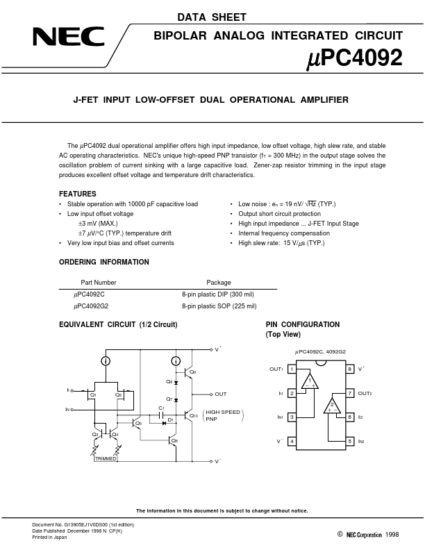
EQUIVALENT CIRCUIT (1/2 Circuit)
+
PIN CONFIGURATION (Top View)
V
µ PC4092C, 4092G2
Q9 Q6 II Q1 Q2 C1 Q5 Q3 Q4 Q8 TRIMMED
−
OUT1
1 1 − +
8
V
+
Q7 Q10
OUT HIGH SPEED PNP
II1
2 2 + −
7
OUT2
IN
D1
IN1
3
6
II2
V
−
4
5
IN2
V
The information in this document is subject to change without notice.
Document No. G13905EJ1V0DS00 (1st edition) Date Published December 1998 N CP(K) Printed in Japan
©
1998
µPC4092
ABSOLUTE MAXIMUM RATINGS (TA = 25 °C)
Parameter
Voltage b...