NEC's NPN SILICON RF TWIN TRANSISTOR
FEATURES
• • • • • LOW VOLTAGE, LOW CURRENT OPERATION LOW CAPACITANCE FOR WIDE TUNI...
NEC's NPN SILICON RF TWIN TRANSISTOR
FEATURES
LOW
VOLTAGE, LOW CURRENT OPERATION LOW CAPACITANCE FOR WIDE TUNING RANGE SMALL PACKAGE OUTLINE: 1.2 mm x 0.8 mm LOW HEIGHT PROFILE: Just 0.50 mm high
0.4 1
UPA861TD
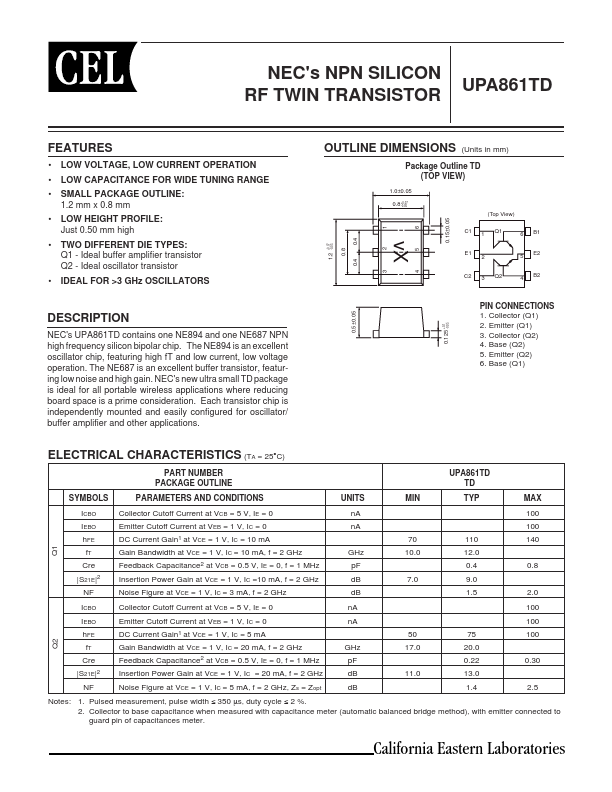
OUTLINE DIMENSIONS
(Units in mm)
Package Outline TD (TOP VIEW)
1.0±0.05 0.8 +0.07 -0.05 (Top View)
0.15±0.05
6
C1
1
Q1
6
B1
vX
3
4
TWO DIFFERENT DIE TYPES: Q1 - Ideal buffer amplifier transistor Q2 - Ideal oscillator transistor IDEAL FOR >3 GHz OSCILLATORS
+0.07 -0.05
2
0.8
5
1.2
E1
0.4
2 Q2
5
E2
C2
3
4
B2
NEC's UPA861TD contains one NE894 and one NE687 NPN high frequency silicon bipolar chip. The NE894 is an excellent oscillator chip, featuring high fT and low current, low
voltage operation. The NE687 is an excellent buffer transistor, featuring low noise and high gain. NEC's new ultra small TD package is ideal for all portable wireless applications where reducing board space is a prime consideration. Each transistor chip is independently mounted and easily configured for oscillator/ buffer amplifier and other applications.
ELECTRICAL CHARACTERISTICS (TA = 25°C)
PART NUMBER PACKAGE OUTLINE SYMBOLS ICBO IEBO hFE PARAMETERS AND CONDITIONS Collector Cutoff Current at VCB = 5 V, IE = 0 Emitter Cutoff Current at VEB = 1 V, IC = 0 DC Current Gain1 at VCE = 1 V, IC = 10 mA Gain Bandwidth at VCE = 1 V, IC = 10 mA, f = 2 GHz Feedback Capacitance2 at VCB = 0.5 V, IE = 0, f = 1 MHz Insertion Power Gain at VCE = 1 V, IC =10 mA, f = 2 GH...