NPN SILICON EPITAXIAL TWIN TRANSISTOR
PRELIMINARY DATA SHEET
NPN SILICON EPITAXIAL TWIN TRANSISTOR
UPA836TC
FEATURES
• SMALL PACKAGE OUTLINE: 1.5 mm x 1.1 ...
Description
PRELIMINARY DATA SHEET
NPN SILICON EPITAXIAL TWIN TRANSISTOR
UPA836TC
FEATURES
SMALL PACKAGE OUTLINE: 1.5 mm x 1.1 mm, 33% smaller than conventional SOT-363 package LOW HEIGHT PROFILE: Just 0.55 mm high FLAT LEAD STYLE: Reduced lead inductance improves electrical performance TWO DIFFERENT DIE TYPES: Q1 - Ideal oscillator transistor Q2 - Ideal buffer amplifier transistor
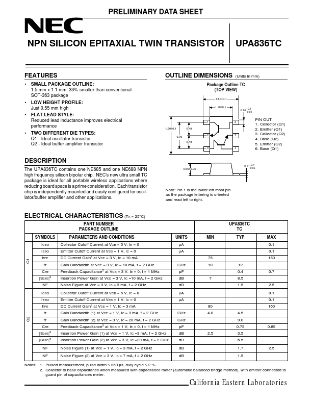
OUTLINE DIMENSIONS
(Units in mm)
Package Outline TC (TOP VIEW)
1.50±0.1 1.10±0.1
0.20 +0.1
-0.05
1 1.50±0.1 0.96 0.48 3 0.48 2
6
5
4
PIN OUT 1. Collector (Q1) 2. Emitter (Q1) 3. Collector (Q2) 4. Base (Q2) 5. Emitter (Q2) 6. Base (Q1)
DESCRIPTION
The UPA836TC contains one NE685 and one NE688 NPN high frequency silicon bipolar chip. NEC's new ultra small TC package is ideal for all portable wireless applications where reducing board space is a prime consideration. Each transistor chip is independently mounted and easily configured for oscillator/buffer amplifier and other applications.
0.55±0.05
0.11+0.1
-0.05
Note: Pin 1 is the lower left most pin as the package lettering is oriented and read left to right.
ELECTRICAL CHARACTERISTICS (TA = 25°C)
PART NUMBER PACKAGE OUTLINE SYMBOLS ICBO IEBO hFE fT Cre |S21E|2 NF ICBO IEBO hFE fT PARAMETERS AND CONDITIONS Collector Cutoff Current at VCB = 5 V, IE = 0 Emitter Cutoff Current at VEB = 1 V, IC = 0 DC Current Gain1 at VCE = 3 V, IC = 10 mA GHz pF dB dB µA µA 80 GHz GHz pF dB dB dB dB 2.5 4.0 4.5 9.0 0.75 3.5 6.5 1.7 1.5 2.5 0.85 7 Gain Band...
Similar Datasheet