DATA SHEET
MOS FIELD EFFECT TRANSISTOR
µPA611TA
N-CHANNEL MOS FIELD EFFECT TRANSISTOR FOR HIGH SPEED SWITCHING
DESCR...
DATA SHEET
MOS FIELD EFFECT TRANSISTOR
µPA611TA
N-CHANNEL MOS FIELD EFFECT TRANSISTOR FOR HIGH SPEED SWITCHING
DESCRIPTION
The µPA611TA is a switching device which can be driven directly by a 2.5-V power source. The µPA611TA has excellent switching characteristics, and is suitable for use as a high-speed switching device in digital circuits.
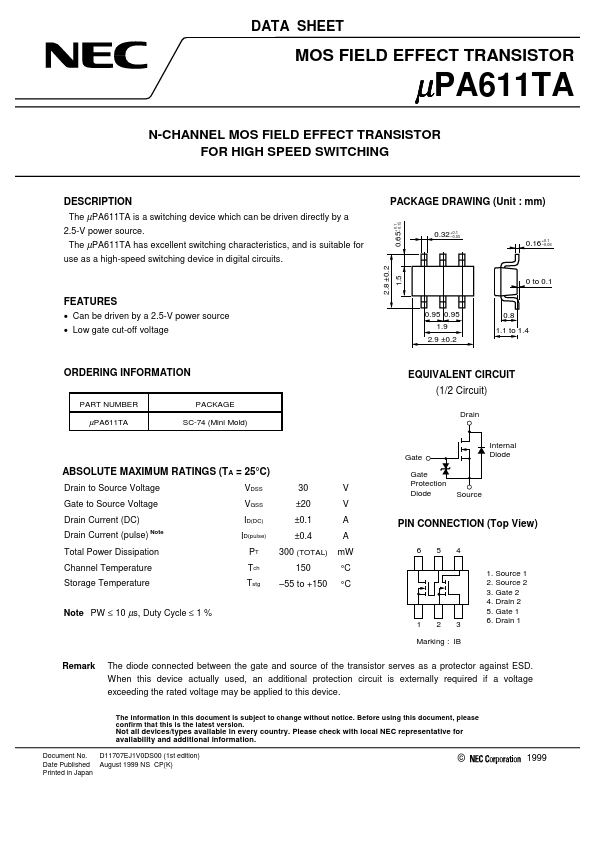
PACKAGE DRAWING (Unit : mm)
0.65 +0.1 –0.15
0.32 +0.1 –0.05 0.16 +0.1 –0.06
2.8 ±0.2
1.5
0 to 0.1
FEATURES
Can be driven by a 2.5-V power source Low gate cut-off
voltage
0.95 0.95 1.9 2.9 ±0.2 0.8 1.1 to 1.4
ORDERING INFORMATION
PART NUMBER PACKAGE
EQUIVALENT CIRCUIT (1/2 Circuit)
µPA611TA
Drain
SC-74 (Mini Mold)
Internal Diode
Gate
ABSOLUTE MAXIMUM RATINGS (TA = 25°C)
Drain to Source
Voltage Gate to Source
Voltage Drain Current (DC) Drain Current (pulse)
Note
VDSS VGSS ID(DC) ID(pulse) PT Tch Tstg
30 ±20 ±0.1 ±0.4 300 (TOTAL) 150 –55 to +150
V V A A mW °C °C
Gate Protection Diode
Source
PIN CONNECTION (Top View)
6 5 4 1. Source 1 2. Source 2 3. Gate 2 4. Drain 2 5. Gate 1 6. Drain 1
Total Power Dissipation Channel Temperature Storage Temperature Note PW ≤ 10 µs, Duty Cycle ≤ 1 %
1
2
3
Marking : IB
Remark
The diode connected between the gate and source of the transistor serves as a protector against ESD. When this device actually used, an additional protection circuit is externally required if a
voltage exceeding the rated
voltage may be applied to this device.
The information in this document is subject t...