DATA SHEET
MOS FIELD EFFECT TRANSISTOR
µ PA1816
P-CHANNEL MOS FIELD EFFECT TRANSISTOR FOR SWITCHING
DESCRIPTION The µPA...
DATA SHEET
MOS FIELD EFFECT TRANSISTOR
µ PA1816
P-CHANNEL MOS FIELD EFFECT TRANSISTOR FOR SWITCHING
DESCRIPTION The µPA1816 is a switching device which can be
driven directly by a 1.8 V power source. This device features a low on-state resistance and
excellent switching characteristics, and is suitable for applications such as power management of notebook computers and so on.
FEATURES 1.8 V drive available Low on-state resistance
RDS(on)1 = 15 mΩ MAX. (VGS = −4.5 V, ID = −4.5 A) RDS(on)2 = 16 mΩ MAX. (VGS = −4.0 V, ID = −4.5 A) RDS(on)3 = 22.5 mΩ MAX. (VGS = −2.5 V, ID = −4.5 A) RDS(on)4 = 41.5 mΩ MAX. (VGS = −1.8 V, ID = −2.5 A) Built-in G-S protection diode against ESD
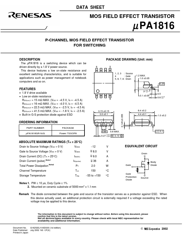
PACKAGE DRAWING (Unit: mm)
85
1, 2, 3 : Source 4 : Gate 5, 6, 7, 8: Drain
1.2 MAX. 1.0 ±0.05
0.25
14
3°
+5° –3°
0.1 ±0.05
0.5
0.6
+0.15 –0.1
3.15 ±0.15 3.0 ±0.1
6.4 ±0.2 4.4 ±0.1
1.0 ±0.2
0.145 ±0.055
ORDERING INFORMATION
PART NUMBER µPA1816GR-9JG
PACKAGE Power TSSOP8
0.65 0.8 MAX.
0.27
+0.03 –0.08
0.10 M
0.1
ABSOLUTE MAXIMUM RATINGS (TA = 25°C)
Drain to Source
Voltage (VGS = 0 V)
VDSS
Gate to Source
Voltage (VDS = 0 V)
VGSS
Drain Current (DC) (TA = 25°C) Drain Current (pulse) Note1 Total Power Dissipation Note2
ID(DC) ID(pulse)
PT
Channel Temperature
Tch
Storage Temperature
Tstg
−12
m 8.0 m 9.0 m 36
2.0
150
−55 to +150
V V A A W °C °C
Notes 1. PW ≤ 10 µs, Duty Cycle ≤ 1% 2. Mounted on ceramic substrate of 5000 mm2 x 1.1 mm
EQUIVALENT CIRCUIT
Drain
Gate
Body Dio...