DATA SHEET
MOS FIELD EFFECT TRANSISTOR
µ PA1756
SWITCHING N-CHANNEL POWER MOS FET INDUSTRIAL USE
DESCRIPTION
This pr...
DATA SHEET
MOS FIELD EFFECT TRANSISTOR
µ PA1756
SWITCHING N-CHANNEL POWER MOS FET INDUSTRIAL USE
DESCRIPTION
This product is Dual N-Channel MOS Field Effect Transistor designed for power management application of notebook computers, and Li-ion battery application.
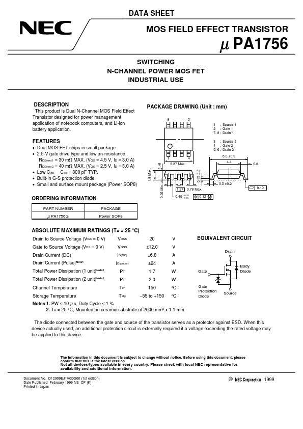
PACKAGE DRAWING (Unit : mm)
8 5 1 ; Source 1 2 ; Gate 1 7, 8 ; Drain 1 3 ; Source 2 4 ; Gate 2 5, 6 ; Drain 2 1 4 5.37 Max.
+0.10 –0.05
FEATURES
Dual MOS FET chips in small package 2.5-V gate drive type and low on-resistance RDS(on)1 = 30 mΩ MAX. (VGS = 4.5 V, ID = 3.0 A) RDS(on)2 = 40 mΩ MAX. (VGS = 2.5 V, ID = 3.0 A) Low Ciss Ciss = 800 pF TYP. Built-in G-S protection diode Small and surface mount package (Power SOP8)
6.0 ±0.3 4.4 0.8
1.8 Max.
1.44
0.15
0.05 Min.
0.5 ±0.2 0.10
1.27 0.40
0.78 Max. 0.12 M
ORDERING INFORMATION
PART NUMBER PACKAGE Power SOP8
+0.10 –0.05
µ PA1756G
ABSOLUTE MAXIMUM RATINGS (TA = 25 °C)
Drain to Source
Voltage (VGS = 0 V) Gate to Source
Voltage (VDS = 0 V) Drain Current (DC) Drain Current (Pulse)Note1 Total Power Dissipation (1 unit)Note2 Total Power Dissipation (2 unit)Note2 Channel Temperature Storage Temperature VDSS VGSS ID(DC) ID(pulse) PT PT Tch Tstg 20 ±12.0 ±6.0 ±24 1.7 2.0 150 −55 to +150 V V A A W W °C °C
Gate Protection Diode Source Gate Drain
EQUIVALENT CIRCUIT
Body Diode
Notes 1. PW ≤ 10 µ s, Duty Cycle ≤ 1 % 2. TA = 25 °C, Mounted on ceramic substrate of 2000 mm2 x 1.1 mm The diode connected between the gate and source of the transistor serves...