DATA SHEET
MOS FIELD EFFECT TRANSISTOR
µ PA1740TP
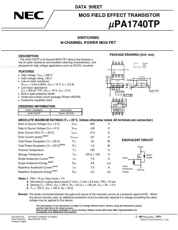
PACKAGE DRAWING (Unit: mm)
8 5 1, 2, 3 : Source 4 : Gate 5, 6, 7, 8,...
DATA SHEET
MOS FIELD EFFECT TRANSISTOR
µ PA1740TP
PACKAGE DRAWING (Unit: mm)
8 5 1, 2, 3 : Source 4 : Gate 5, 6, 7, 8, 9 : Drain
SWITCHING N-CHANNEL POWER MOS FET
The µPA1740TP is N-channel MOS FET device that features a low on-state resistance and excellent swiching characteristics, and designed for high
voltage applications such as DC/DC converter. www.DataSheet4U.com
DESCRIPTION
FEATURES
High
voltage: VDSS = 200 V Gate
voltage rating: ±30 V Low on-state resistance RDS(on) = 0.44 Ω MAX. (VGS = 10 V, ID = 3.5 A) Low input capacitance Ciss = 420 pF TYP. (VDS = 10 V, VGS = 0 V) Built-in gate protection diode Small and surface mount package (Power HSOP8) Avalanche capability rated
1.49 ±0.21 1.44 TYP.
1 5.2 +0.17 –0.2 4 0.8 ±0.2 S
+0.10 –0.05
6.0 ±0.3 4.4 ±0.15
0.05 ±0.05
0.15
1.27 TYP. 0.40
1
+0.10 –0.05
0.10 S 0.12 M
2.0 ±0.2
2.9 MAX.
ORDERING INFORMATION
PART NUMBER µPA1740TP PACKAGE Power HSOP8
8
9 4.1 MAX.
5
ABSOLUTE MAXIMUM RATINGS (TA = 25°C, Unless otherwise noted, All terminals are connected.)
Drain to Source
Voltage (VGS = 0 V) Gate to Source
Voltage (VDS = 0 V) Drain Current (DC) (TC = 25°C) Drain Current (pulse)
Note1
VDSS VGSS ID(DC) ID(pulse) PT1 PT2 Tch Tstg
Note2
200 ±30 ±7.0 ±21 22 1.0 150 –55 to + 150 7.0 4.9 7.0 2.2
V V A A W W °C °C A mJ A mJ
Gate Protection Diode Source Gate Body Diode
Total Power Dissipation (TC = 25°C) Total Power Dissipation (TA = 25°C) Channel Temperature Storage Temperature Single Avalanche Current Si...