DATA SHEET
MOS FIELD EFFECT TRANSISTOR
µPA1728
SWITCHING N-CHANNEL POWER MOS FET INDUSTRIAL USE
DESCRIPTION
The µPA1...
DATA SHEET
MOS FIELD EFFECT TRANSISTOR
µPA1728
SWITCHING N-CHANNEL POWER MOS FET INDUSTRIAL USE
DESCRIPTION
The µPA1728 is N-Channel MOS Field Effect Transistor designed for high current switching applications.
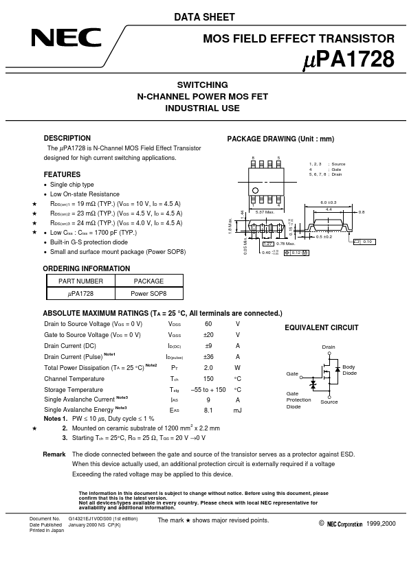
PACKAGE DRAWING (Unit : mm)
8 5 1, 2, 3 ; Source 4 ; Gate 5, 6, 7, 8 ; Drain
FEATURES
Single chip type Low On-state Resistance 5 5 5 5 RDS(on)1 = 19 mΩ (TYP.) (VGS = 10 V, ID = 4.5 A)
1.44
1 5.37 Max.
+0.10 –0.05
4
6.0 ±0.3 4.4 0.8
RDS(on)2 = 23 mΩ (TYP.) (VGS = 4.5 V, ID = 4.5 A) RDS(on)3 = 24 mΩ (TYP.) (VGS = 4.0 V, ID = 4.5 A) Low Ciss : Ciss = 1700 pF (TYP.) Built-in G-S protection diode Small and surface mount package (Power SOP8)
1.8 Max.
0.15
0.05 Min.
0.5 ±0.2 0.10
1.27 0.40
0.78 Max. 0.12 M
+0.10 –0.05
ORDERING INFORMATION
PART NUMBER PACKAGE Power SOP8
µPA1728
ABSOLUTE MAXIMUM RATINGS (TA = 25 °C, All terminals are connected.)
Drain to Source
Voltage (VGS = 0 V) Gate to Source
Voltage (VDS = 0 V) Drain Current (DC) Drain Current (Pulse)
Note1 Note2
VDSS VGSS ID(DC) ID(pulse) PT Tch Tstg
60 ±20 ±9 ±36 2.0 150 –55 to + 150 9 8.1
2
V V A A W
EQUIVALENT CIRCUIT
Drain
Total Power Dissipation (TA = 25 °C) Channel Temperature Storage Temperature Single Avalanche Current
Note3 Note3
Gate
Body Diode
°C °C A mJ
Gate Protection Diode
IAS EAS
Source
Single Avalanche Energy Notes 1. PW ≤ 10 µs, Duty cycle ≤ 1 % 5
2. Mounted on ceramic substrate of 1200 mm x 2.2 mm 3. Starting Tch = 25°C, RG = 25 Ω, TGS = 20 V →0 V Remark The diode c...