DATA SHEET
COMPOUND FIELD EFFECT POWER TRANSISTOR
µPA1552B
N-CHANNEL POWER MOS FET ARRAY SWITCHING USE
DESCRIPTION
Th...
DATA SHEET
COMPOUND FIELD EFFECT POWER TRANSISTOR
µPA1552B
N-CHANNEL POWER MOS FET ARRAY SWITCHING USE
DESCRIPTION
The µPA1552B is N-channel Power MOS FET Array that built in 4 circuits designed, for solenoid, motor and lamp driver.
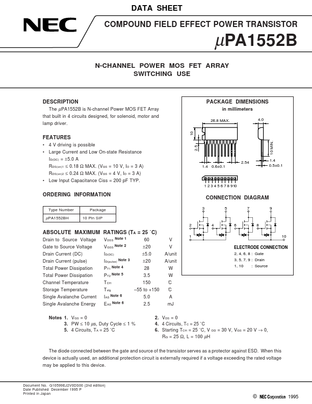
PACKAGE DIMENSIONS
in millimeters
26.8 MAX.
10
4.0
FEATURES
Large Current and Low On-state Resistance ID(DC) = ± 5.0 A RDS(on)1 ≤ 0.18 Ω MAX. (VGS = 10 V, ID = 3 A) RDS(on)2 ≤ 0.24 Ω MAX. (VGS = 4 V, ID = 3 A) Low Input Capacitance Ciss = 200 pF TYP.
1 2 3 4 5 6 7 8 9 10 1.4 0.6±0.1
2.5
4 V driving is possible
2.54
1.4 0.5±0.1
ORDERING INFORMATION
Type Number Package 10 Pin SIP
2 3
CONNECTION DIAGRAM
5 7 9
µPA1552BH
4
6
8 10
ABSOLUTE MAXIMUM RATINGS (TA = 25 ˚C)
Drain to Source
Voltage Gate to Source
Voltage Drain Current (DC) Drain Current (pulse) Total Power Dissipation Total Power Dissipation Channel Temperature Storage Temperature Single Avalanche Current Single Avalanche Energy VDSS Note 1 VGSS Note 2 ID(DC) ID(pulse) Note 3 PT1 Note 4 PT2 Note 5 TCH Tstg IAS Note 6 EAS Note 6 60 ± 20 ± 5.0 ± 20 28 3.5 150 –55 to +150 5.0 2.5 V V A/unit A/unit W W ˚ C ˚ C A mJ
1
ELECTRODE CONNECTION 2, 4, 6, 8 : Gate 3, 5, 7, 9 : Drain 1, 10 : Source
Notes 1. VGS = 0 3. PW ≤ 10 µs, Duty Cycle ≤ 1 % 5. 4 Circuits, TA = 25 ˚C
2. VDS = 0 4. 4 Circuits, TC = 25 ˚C 6. Starting TCH = 25 ˚C, V DD = 30 V, VGS = 20 V → 0, RG = 25 Ω, L = 100 µH
The diode connected between the gate and source of the transistor serves as a protector against ESD...