*
e-5 -,--5 3 .---= = = -a== =- an AMP company
RF MOSFET Power Transistor, IOOW, 28V 100 - 500 MHz
Features
l l l l l
...
*
e-5 -,--5 3 .---= = = -a== =- an AMP company
RF
MOSFET Power Transistor, IOOW, 28V 100 - 500 MHz
Features
l l l l l
UF281 OOV
v2.00
N-Channel Enhancement DMOS Structure Lower Capacitances Lower
&lode Device Operation
for Broadband
High Saturated Output Power
Noise Figure Than Competitive Devices
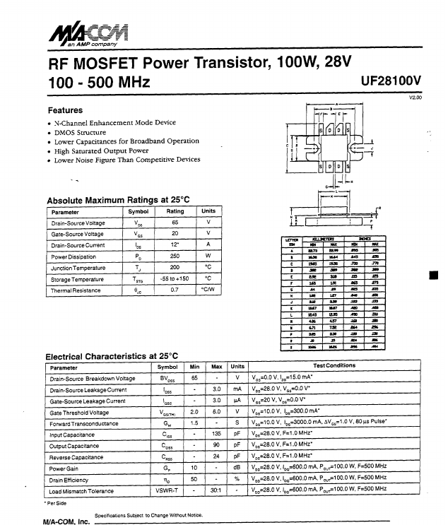
Absolute Maximum Ratings at 25°C
I Parameter Drain-Source
Voltage Gate-Source
Voltage Drain-Source Current ( Symbol V DS V GS ‘DS 1 Rating 65 20 12 250 200 -55 to +150 0.7 ( Units
V V
A
Power Dissipation JunctionTemperature Storage Temperature Thermal Resistance
PD
TJ T sic 8 IP
W
“C “C “crw
Electrical _____.._~~
Parameter Drain-Source Drain-Source Gate-Source
Characteristics at 25°C
Symbol Breakdown Min Max Units lest Conditions
Voltage
BV,,,
IDSS ‘GSS
65 ,
2.0 1.5 -
3.0 ) 3.0 6.0 135 90 24 ] I
V mA
fl
V,.=O.O V. I& V,,=28.0 ,
1 v,,=2ov, I
5.0 mA
LeakageCurrent Leakage Current
V, V,,=O.O V’
vDs=o.o v
Gate Threshold
Voltage ForwardTransconductance input Capacitance Output Capacitance Reverse Capacitance Power Gain Drain Efficiency . Load Mismatch Tolerance - Per Side
V GSIW
GM c 15s C ass
V
S pF PF pF dB % -
V,,=lO.O
V, 1,,=300.0
V, 1,,=3000.0
mA‘
mA, AV,,=l .O V, 80 us Pulse’
V,,=10.0 V,,=28.0 V,,=28.0 V,,=28.0 V,,=28.0 V,,=28.0 V,,=28.0
V, F=l .O MHz’ V, F=l .O MHz’ V, F=l .O MHz’ V, 1,,=600.0 mA, P,,$OO.O W, F=SOO MHz
C RSS GP
10 50
3O:l
V, 1,,=600.0
mA, P,,,=lOO.O W. F=500 MHZ
W, F=500 MHz
VSWR-T
-
V, lDD=800.0 mA, PbbylOO.0
Specifications...