U1898
U1898
N-Channel Switch
• This device is designed for low level analog switching, sample and hold circuits and cho...
U1898
U1898
N-Channel Switch
This device is designed for low level analog switching, sample and hold circuits and chopper stabalized
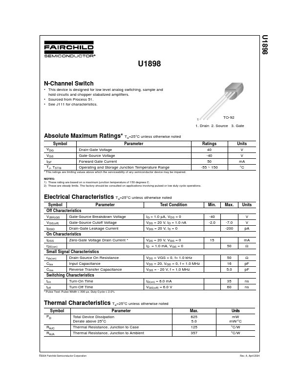
amplifiers. Sourced from Process 51. See J111 for characteristics. TO-92
1
1. Drain 2. Source 3. Gate
Absolute Maximum Ratings* Ta=25°C unless otherwise noted
Symbol VDG VGS IGF TJ, TSTG Parameter Drain-Gate
Voltage Gate-Source
Voltage Forward Gate Current Operating and Storage Junction Temperature Range Ratings 40 -40 50 -55 ~ 150 Units V V mA °C
* This ratings are limiting values above which the serviceability of any semiconductor device may be impaired. NOTES: 1) These rating are based on a maximum junction temperature of 150 degrees C. 2) These are steady limits. The factory should be consulted on applications involving pulsed or low duty cycle operations.
Electrical Characteristics Ta=25°C unless otherwise noted
Symbol Off Characteristics V(BR)GS VGS(off) IDGO IDSS rDS(on) Small Signal Characteristics rds(on) Ciss Crss ton toff Drain-Source On Resistance Input Capacitance Reverse Transfer Capacitance Turn-On Time Turn-Off Time VDS = VGS = 0, f= 1.0 kHz VDS = 20, VGS = 0, f = 1.0 MHz VGS = - 20 V, f = 1.0 MHz ID(on) = 6.0 mA VGS(off) = 6.0 V 50 16 5.0 35 60 Ω pF pF ns ns Parameter Test Condition IG = 1.0 µA, VDS = 0 VDS = 20 V, ID = 1.0 nA VDG = 20 V, IS = 0 VDS = 20 V, VGS = 0 ID = 1.0 mA, VGS = 0 15 50 Min. -40 -2.0 -7.0 -200 Max. Units V V pA mA Ω Gate-Source Breakdown
Voltage Gate-Source Cutoff
Voltage Drain-Gate Leakage Curr...