TC4081BP/BF
TOSHIBA CMOS Digital Integrated Circuit Silicon Monolithic
TC4081BP, TC4081BF
TC4081B Quad 2-Input AND Gate
...
TC4081BP/BF
TOSHIBA
CMOS Digital Integrated Circuit Silicon Monolithic
TC4081BP, TC4081BF
TC4081B Quad 2-Input AND Gate
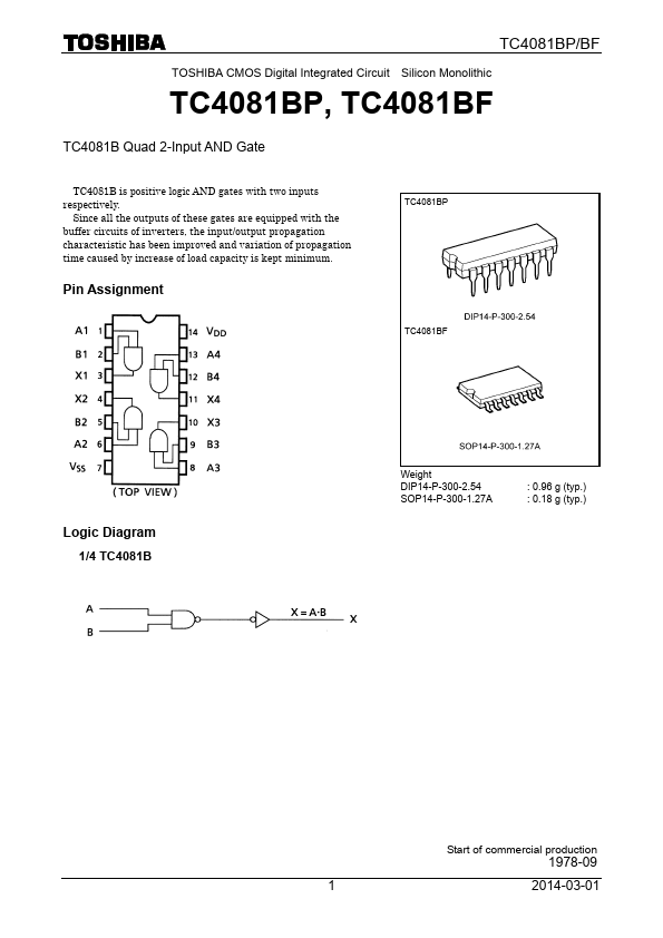
TC4081B is positive logic AND gates with two inputs respectively.
Since all the outputs of these gates are equipped with the buffer circuits of inverters, the input/output propagation characteristic has been improved and variation of propagation time caused by increase of load capacity is kept minimum.
Pin Assignment
TC4081BP
TC4081BF
Logic Diagram
1/4 TC4081B
Weight DIP14-P-300-2.54 SOP14-P-300-1.27A
: 0.96 g (typ.) : 0.18 g (typ.)
Start of commercial production
1978-09
1
2014-03-01
TC4081BP/BF
Absolute Maximum Ratings (Note)
Characteristics
Symbol
Rating
Unit
DC supply
voltage Input
voltage Output
voltage DC input current Power dissipation Operating temperature range Storage temperature range
VDD VIN VOUT IIN PD Tope Tstg
VSS − 0.5 to VSS + 20
V
VSS − 0.5 to VDD + 0.5
V
VSS − 0.5 to VDD + 0.5
V
±10
mA
300 (DIP)/180 (SOIC)
mW
−40 to 85
°C
−65 to 150
°C
Note:
Exceeding any of the absolute maximum ratings, even briefly, lead to deterioration in IC performance or even destruction. Using continuously under heavy loads (e.g. the application of high temperature/current/
voltage and the significant change in temperature, etc.) may cause this product to decrease in the reliability significantly even if the operating conditions (i.e. operating temperature/current/
voltage, etc.) are within the absolute maximum ratings and the operating...