www.DataSheet4U.com
N-CHANNEL 600V - 0.48Ω - 12A TO-247 PowerMesh™ II MOSFET
TYPE STW12NC60
s s s s s
STW12NC60
VDSS ...
www.DataSheet4U.com
N-CHANNEL 600V - 0.48Ω - 12A TO-247 PowerMesh™ II
MOSFET
TYPE STW12NC60
s s s s s
STW12NC60
VDSS 600V
RDS(on) < 0.55Ω
ID 12 A
TYPICAL RDS(on) = 0.48Ω EXTREMELY HIGH dv/dt CAPABILITY 100% AVALANCHE TESTED NEW HIGH
VOLTAGE BENCHMARK GATE CHARGE MINIMIZED
1
3 2
DESCRIPTION The PowerMESH™ II is the evolution of the first generation of MESH OVERLAY™ . The layout refinements introduced greatly improve the Ron*area figure of merit while keeping the device at the leading edge for what concerns swithing speed, gate charge and ruggedness. APPLICATIONS s SWITCH MODE POWER SUPPLIES (SMPS) s HIGH CURRENT, HIGH SPEED SWITCHING s DC-AC CONVERTERS FOR WELDING EQUIPMENT AND UNINTERRUPTIBLE POWER SUPPLIES AND MOTOR DRIVE
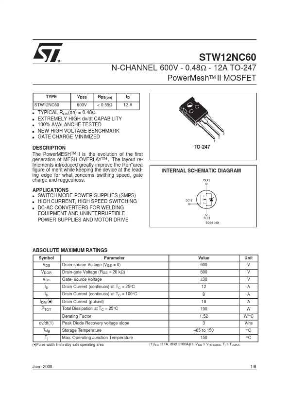
TO-247
INTERNAL SCHEMATIC DIAGRAM
ABSOLUTE MAXIMUM RATINGS
Symbol VDS VDGR VGS ID ID IDM (q) PTOT dv/dt(1) Tstg Tj Parameter Drain-source
Voltage (VGS = 0) Drain-gate
Voltage (RGS = 20 kΩ) Gate- source
Voltage Drain Current (continuos) at TC = 25°C Drain Current (continuos) at TC = 100° C Drain Current (pulsed) Total Dissipation at TC = 25°C Derating Factor Peak Diode Recovery
voltage slope Storage Temperature Max. Operating Junction Temperature Value 600 600 ±30 12 8 18 190 1.52 3 –65 to 150 150
(1)ISD ≤11A, di/dt ≤100A/µ s, V DD ≤ V(BR)DSS, Tj ≤ TJMAX.
Unit V V V A A A W W/ °C V/ns °C °C
()Pulse width limited by safe operating area
June 2000
1/8
STW12NC60
THERMAL DATA
Rthj-case Rthj-amb Rthc-sink Tl Thermal Resistance Junction-case Max Th...