www.DataSheet4U.com
STW12NA50
N - CHANNEL ENHANCEMENT MODE FAST POWER MOS TRANSISTOR
TYPE STW12NA50
s s s s s s s
V DS...
www.DataSheet4U.com
STW12NA50
N - CHANNEL ENHANCEMENT MODE FAST POWER MOS TRANSISTOR
TYPE STW12NA50
s s s s s s s
V DSS 500 V
R DS( on) < 0.6 Ω
ID 11.6 A
TYPICAL RDS(on) = 0.5 Ω ± 30V GATE TO SOURCE
VOLTAGE RATING 100% AVALANCHE TESTED REPETITIVE AVALANCHE DATA AT 100oC LOW INTRINSIC CAPACITANCES GATE GHARGE MINIMIZED REDUCED THRESHOLD
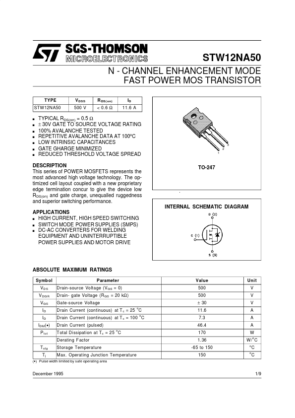
VOLTAGE SPREAD TO-247
3 2 1
DESCRIPTION This series of POWER
MOSFETS represents the most advanced high
voltage technology. The optimized cell layout coupled with a new proprietary edge termination concur to give the device low RDS(on) and gate charge, unequalled ruggedness and superior switching performance. APPLICATIONS s HIGH CURRENT, HIGH SPEED SWITCHING s SWITCH MODE POWER SUPPLIES (SMPS) s DC-AC CONVERTERS FOR WELDING EQUIPMENT AND UNINTERRUPTIBLE POWER SUPPLIES AND MOTOR DRIVE
INTERNAL SCHEMATIC DIAGRAM
ABSOLUTE MAXIMUM RATINGS
Symbol VD S V DG R V GS ID ID ID M( ) P tot T stg Tj Parameter Drain-source
Voltage (V GS = 0) Drain- gate
Voltage (R GS = 20 kΩ ) Gate-source
Voltage Drain Current (continuous) at T c = 25 C Drain Current (continuous) at T c = 100 oC Drain Current (pulsed) Total Dissipation at Tc = 25 C Derating Factor Storage Temperature Max. Operating Junction Temperature
o o
Value 500 500 ± 30 11.6 7.3 46.4 170 1.36 -65 to 150 150
Unit V V V A A A W W/o C
o o
C C
() Pulse width limited by safe operating area
December 1995
1/9
STW12NA50
THERMAL DATA
R thj-cas e Rthj- amb Rthj- amb Tl Thermal Resistance Junction...