N-CHANNEL 150V - 0.085 Ω - 10A TO-220FP MESH OVERLAY™ POWER MOSFET
TYPE STP30NS15LFP
s s s
STP30NS15LFP
VDSS 150 V
RD...
N-CHANNEL 150V - 0.085 Ω - 10A TO-220FP MESH OVERLAY™ POWER
MOSFET
TYPE STP30NS15LFP
s s s
STP30NS15LFP
VDSS 150 V
RDS(on) <0.1Ω
ID 10 A
TYPICAL RDS(on) = 0.085Ω EXTREMELY HIGH dv/dt CAPABILITY 100% AVALANCHE TESTED
DESCRIPTION
Using the latest high
voltage MESH OVERLAY™ process, STMicroelectronics has designed an advanced family of power
MOSFETs with outstanding performances. The new patent pending strip layout coupled with the Company’s proprietary edge termination structure, gives the lowest RDS(on) per area, exceptional avalanche and dv/dt capabilities and unrivalled gate charge and switching characteristics.
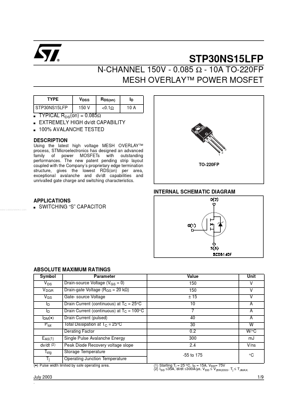
3 1 2
TO-220FP
INTERNAL SCHEMATIC DIAGRAM APPLICATIONS s SWITCHING “S” CAPACITOR
www.DataSheet4U.com
ABSOLUTE MAXIMUM RATINGS
Symbol VDS VDGR VGS ID ID IDM() Ptot EAS(1) dv/dt (2) Tstg Tj Parameter Drain-source
Voltage (VGS = 0) Drain-gate
Voltage (RGS = 20 kΩ) Gate- source
Voltage Drain Current (continuous) at TC = 25°C Drain Current (continuous) at TC = 100°C Drain Current (pulsed) Total Dissipation at TC = 25°C Derating Factor Single Pulse Avalanche Energy Peak Diode Recovery
voltage slope Storage Temperature Operating Junction Temperature Value 150 150 ± 15 10 7 40 30 0.2 300 2.4 -55 to 175
(1) Starting T j = 25 oC, ID = 15A, VDD= 75V (2) ISD ≤35A, di/dt ≤300A/µs, VDD ≤ V(BR)DSS, Tj ≤ TJMAX.
Unit V V V A A A W W/°C mJ V/ns °C
() Pulse width limited by safe operating area. July 2003
.
1/9
STP30NS15LFP
THERMAL DATA
Rthj-case Rthj-amb Tl Thermal Resi...