®
STP20NE10
N - CHANNEL 100V - 0.07Ω - 20A - TO-220 STripFET™ MOSFET
TYPE ST P20NE10
s s s s
V DSS 100 V
R DS(on) < ...
®
STP20NE10
N - CHANNEL 100V - 0.07Ω - 20A - TO-220 STripFET™
MOSFET
TYPE ST P20NE10
s s s s
V DSS 100 V
R DS(on) < 0.1 Ω
ID 20 A
TYPICAL RDS(on) = 0.07 Ω EXCEPTIONAL dv/dt CAPABILITY 100% AVALANCHE TESTED APPLICATION ORIENTED CHARACTERIZATION
2 3
DESCRIPTION This Power
MOSFET is the latest development of SGS-THOMSON unique ”Single Feature Size™ ” strip-based process.The resulting transistor shows extremely high packing density for low onresistance, rugged avalanche characteristics and less critical alignment steps therefore a remarkable manufacturing reproducibility. APPLICATIONS s SOLENOID AND RELAY DRIVERS s MOTOR CONTROL, AUDIO
AMPLIFIERS s DC-DC CONVERTERS s AUTOMOTIVE ENVIRONMENT
1
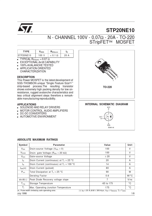
TO-220
INTERNAL SCHEMATIC DIAGRAM
ABSOLUTE MAXIMUM RATINGS
Symbol V DS V DGR V GS ID ID IDM ( ) P t ot Parameter Drain-source
Voltage (V GS = 0) Drain- gate
Voltage (R GS = 20 k Ω ) Gate-source
Voltage Drain Current (continuous) at Tc = 25 C Drain Current (continuous) at Tc = 100 oC Drain Current (pulsed) Total Dissipation at Tc = 25 C Derating F actor dv/dt( 1 ) T stg Tj July 1998 Peak Diode Recovery
voltage slope Storage T emperature Max. O perating Junction Temperature
o o
Value 100 100 ± 20 20 14 80 90 0.6 7 -65 to 175 175
( 1) ISD ≤ 20 A, di/dt ≤ 300 A/µs, VDD ≤ V(BR)DSS, Tj ≤ TJMAX
Uni t V V V A A A W W/ o C V/ ns
o o
C C 1/8
() Pulse width limited by safe operating area
STP20NE10
THERMAL DATA
R t hj-ca se
Rthj -amb
R thc- si nk Tl
Thermal Resistance Junction-case M...