®
STP20NE06 STP20NE06FP
N - CHANNEL 60V - 0.06 Ω - 20A TO-220/TO-220FP STripFET™ POWER MOSFET
TYPE STP20NE06 STP20NE06...
®
STP20NE06 STP20NE06FP
N - CHANNEL 60V - 0.06 Ω - 20A TO-220/TO-220FP STripFET™ POWER
MOSFET
TYPE STP20NE06 STP20NE06FP
s s s s s
V DSS 60 V 60 V
R DS(on) < 0.080 Ω < 0.080 Ω
ID 20 A 13 A
TYPICAL RDS(on) = 0.06 Ω EXCEPTIONAL dv/dt CAPABILITY 100% AVALANCHE TESTED LOW GATE CHARGE 100 oC APPLICATION ORIENTED CHARACTERIZATION
1
3 2
1 2
3
DESCRIPTION This Power
Mosfet is the latest development of STMicroelectronics unique ” Single Feature Size™ ” strip-based process. The resulting transistor shows extremely high packing density for low on-resistance, rugged avalance characteristics and less critical alignment steps therefore a remarkable manufacturing reproducibility. APPLICATIONS s HIGH CURRENT, HIGH SPEED SWITCHING s SOLENOID AND RELAY DRIVERS s MOTOR CONTROL, AUDIO
AMPLIFIERS s DC-DC & DC-AC CONVERTERS s AUTOMOTIVE ENVIRONMENT (INJECTION, ABS, AIR-BAG, LAMPDRIVERS, Etc.)
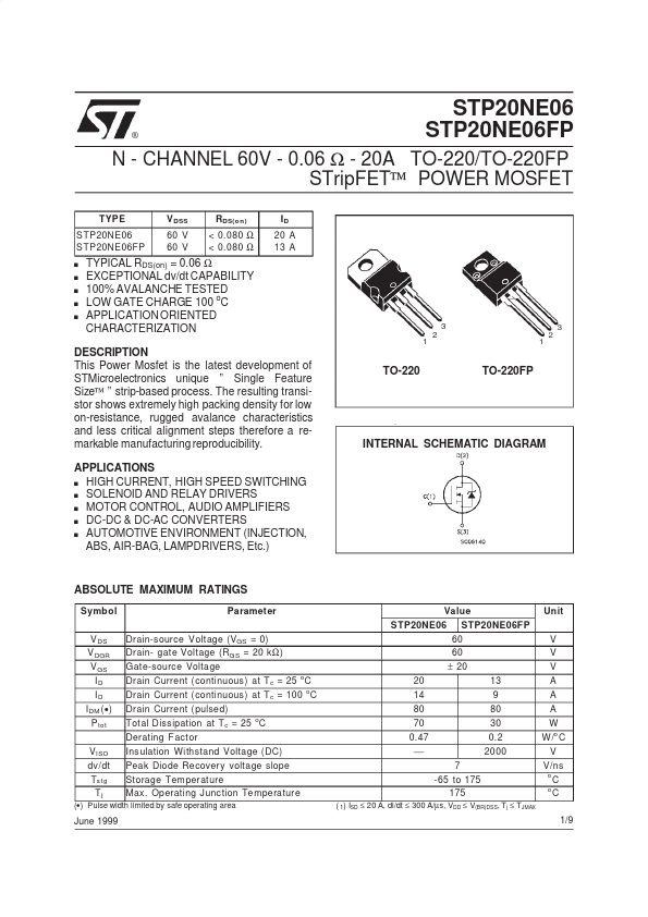
TO-220
TO-220FP
INTERNAL SCHEMATIC DIAGRAM
ABSOLUTE MAXIMUM RATINGS
Symbol V DS V DGR V GS ID ID I DM ( ) P tot V ISO dv/dt Ts tg Tj June 1999 Parameter Drain-source
Voltage (VGS = 0) Drain- gate
Voltage (RGS = 20 k Ω ) Gate-source
Voltage Drain Current (continuous) at T c = 25 o C Drain Current (continuous) at T c = 100 oC Drain Current (pulsed) Total Dissipation at T c = 25 oC Derating F actor Insulation Withstand
Voltage (DC) Peak Diode Recovery
voltage slope Storage Temperature Max. Operating Junction Temperature 20 14 80 70 0.47 7 -65 to 175 175
( 1) ISD ≤ 20 A, di/dt ≤ 300 A/µs, VDD ≤ V...