STB12NM60N/-1 - STF12NM60N STP12NM60N - STW12NM60N
N-channel 600V - 0.35Ω - 10A - D2/I2PAK - TO-220/FP - TO-247 Second g...
STB12NM60N/-1 - STF12NM60N STP12NM60N - STW12NM60N
N-channel 600V - 0.35Ω - 10A - D2/I2PAK - TO-220/FP - TO-247 Second generation MDmesh™ Power
MOSFET
Features
www.DataSheet4U.com
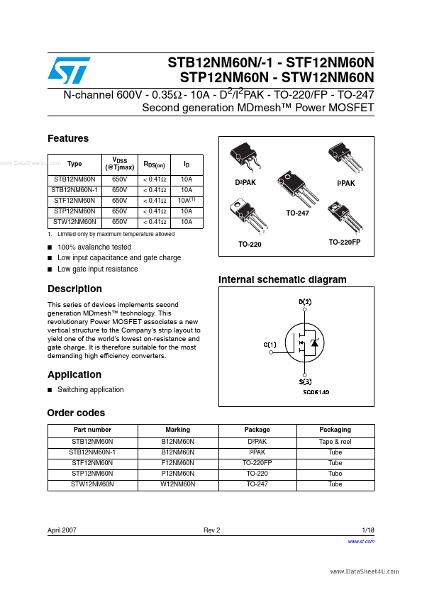
Type
VDSS (@Tjmax) 650V 650V 650V 650V 650V
RDS(on) < 0.41Ω < 0.41Ω < 0.41Ω < 0.41Ω < 0.41Ω
ID
1
3
3 12
STB12NM60N STB12NM60N-1 STF12NM60N STP12NM60N STW12NM60N
10A 10A 10A(1) 10A 10A
D²PAK
I²PAK
TO-247
3 1 2
3 1 2
1. Limited only by maximum temperature allowed ■ ■ ■
100% avalanche tested Low input capacitance and gate charge Low gate input resistance
TO-220
TO-220FP
Internal schematic diagram Description
This series of devices implements second generation MDmesh™ technology. This revolutionary Power
MOSFET associates a new vertical structure to the Company’s strip layout to yield one of the world’s lowest on-resistance and gate charge. It is therefore suitable for the most demanding high efficiency converters.
Application
■
Switching application
Order codes
Part number STB12NM60N STB12NM60N-1 STF12NM60N STP12NM60N STW12NM60N Marking B12NM60N B12NM60N F12NM60N P12NM60N W12NM60N Package D²PAK I²PAK TO-220FP TO-220 TO-247 Packaging Tape & reel Tube Tube Tube Tube
April 2007
Rev 2
1/18
www.st.com 18
Contents
STB12NM60N/-1 - STF12NM60N - STP12NM60N - STW12NM60N
Contents
1 2 Electrical ratings . . . . . . . . . . . . . . . . . . . . . . . . . . . . . . . . . . . . . . . . . . . . 3 Electrical characteristics . . . . . . . . . . . . . . . . . . . . . . . . . . . . . . . . . . . . ...