STD840DN40
Dual NPN high voltage transistors in a single package
Preliminary data
Features
■ ■ ■ ■
Low VCE(sat) Simpli...
STD840DN40
Dual NPN high
voltage transistors in a single package
Preliminary data
Features
■ ■ ■ ■
Low VCE(sat) Simplified circuit design Reduced component count Fast switching speed
8 4 1
Applications
■ ■
Compact fluorescent lamp (CFL) 220 V mains Electronic ballast for fluorescent lighting
DIP-8
Description
The device is a dual NPN high
voltage power transistors manufactured in multi-epitaxial planar technology. It is housed in dual island DIP-8 package with separated terminals for high assembly flexibility.
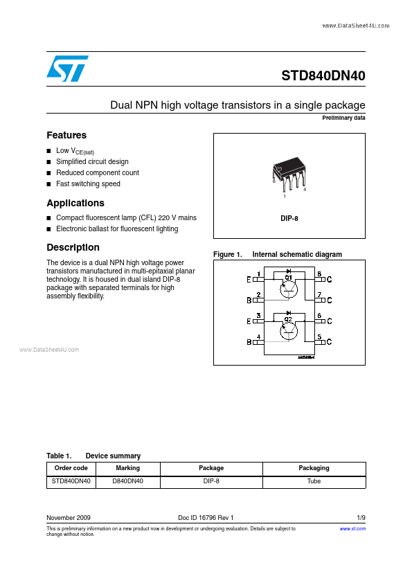
Figure 1.
Internal schematic diagram
www.DataSheet4U.com
Table 1.
Device summary
Marking D840DN40 Package DIP-8 Packaging Tube
Order code STD840DN40
November 2009
Doc ID 16796 Rev 1
1/9
www.st.com 9
This is preliminary information on a new product now in development or undergoing evaluation. Details are subject to change without notice.
Electrical ratings
STD840DN40
1
Electrical ratings
Table 2.
Symbol VCBO VCEO VEBO IC ICM IB IBM PTOT TSTG TJ
Absolute maximum ratings
Parameter Collector-base
voltage (IE = 0) Collector-emitter
voltage (IB = 0) Emitter-base
voltage (IC = 0, IB = 1.5 A, tp < 10 ms) Collector current Collector peak current (tP < 5 ms) Base current Base peak current (tP < 5 ms) Total dissipation at Tamb = 25 °C single transistor Total dissipation at Tamb = 25 °C both transistors Storage temperature Max. operating junction temperature Value 700 400 V(BR)EBO 4 8 1.5 3 TBD TBD -65 to 150 150 Unit V V V A A A A W W °C °C
Table 3.
Symbol Rt...