www.DataSheet4U.com
N-CHANNEL 40V - 3.9 mΩ - 120A D2PAK/I2PAK/TO-220 STripFET™ II POWER MOSFET
TYPE STB190NF04/-1 STP19...
www.DataSheet4U.com
N-CHANNEL 40V - 3.9 mΩ - 120A D2PAK/I2PAK/TO-220 STripFET™ II POWER
MOSFET
TYPE STB190NF04/-1 STP190NF04
s s s
STP190NF04 STB190NF04 STB190NF04-1
PRELIMINARY DATA
VDSS 40 V 40 V
RDS(on) <0.0043 Ω <0.0043 Ω
ID 120 A 120 A
3 1
TYPICAL RDS(on) =3.9 mΩ STANDARD THRESHOLD DRIVE 100% AVALANCHE TESTED
3 12
DESCRIPTION This Power
MOSFET is the latest development of STMicroelectronis unique "Single Feature Size™" strip-based process. The resulting transistor shows extremely high packing density for low onresistance, rugged avalanche characteristics and less critical alignment steps therefore a remarkable manufacturing reproducibility. APPLICATIONS s HIGH CURENT, HIGH SWITCHING SPEED s AUTOMOTIVE
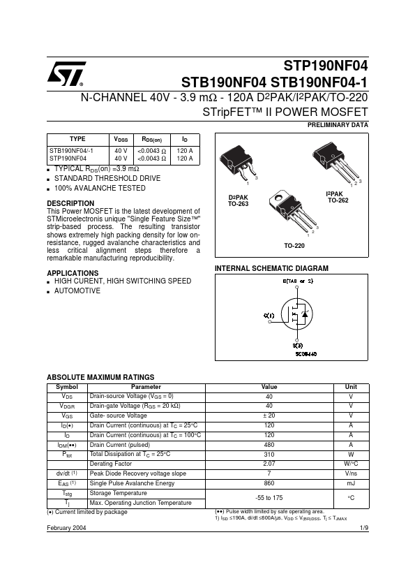
D2PAK TO-263
I2PAK TO-262
3 1 2
TO-220
INTERNAL SCHEMATIC DIAGRAM
ABSOLUTE MAXIMUM RATINGS
Symbol VDS VDGR VGS ID() ID IDM() Ptot dv/dt
(1)
Parameter Drain-source
Voltage (VGS = 0) Drain-gate
Voltage (RGS = 20 kΩ) Gate- source
Voltage Drain Current (continuous) at TC = 25°C Drain Current (continuous) at TC = 100°C Drain Current (pulsed) Total Dissipation at TC = 25°C Derating Factor Peak Diode Recovery
voltage slope Single Pulse Avalanche Energy Storage Temperature Max. Operating Junction Temperature
Value 40 40 ± 20 120 120 480 310 2.07 7 860 -55 to 175 () Pulse width limited by safe operating area.
Unit V V V A A A W W/°C V/ns mJ °C
EAS (1) Tstg Tj
() Current limited by package
February 2004
1) ISD ≤190A, di/dt ≤600A/µs, VDD ≤ V(BR)DSS, Tj ≤ TJMA...