www.DataSheet4U.com
P Channel Enchancement Mode MOSFET -1.7A DESCRIPTION
ST2303
The ST2303 is the P-Channel logic enh...
www.DataSheet4U.com
P Channel Enchancement Mode
MOSFET -1.7A DESCRIPTION
ST2303
The ST2303 is the P-Channel logic enhancement mode power field effect transistor are produced using high cell density, DMOS trench technology. This high density process is especially tailored to minimize on-state resistance. These devices are particularly suited for low
voltage application such as cellular phone and notebook computer power management and other batter powered circuits, and low in-line power loss are needed in a very small outine surface mount package.
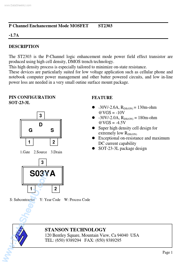
PIN CONFIGURATION SOT-23-3L 3
FEATURE z -30V/-2.6A, RDS(ON) = 130m-ohm @VGS = -10V z -30V/-2.0A, RDS(ON) = 180m-ohm @VGS = -4.5V z Super high density cell design for extremely low RDS(ON) z Exceptional on-resistance and maximum DC current capability z SOT-23-3L package design
D G
1
1.Gate 2.Source
S
2
3.Drain
3
ata
Sh
eet
S: Subcontractor
4U
1
.co
m
S03YA
2
W: Process Code
Y: Year Code
STANSON TECHNOLOGY
120 Bentley Square, Mountain View, Ca 94040 USA TEL: (650) 9389294 FAX: (650) 9389295
Page 1
ww
w.D
www.DataSheet4U.com
P Channel Enchancement Mode
MOSFET -1.7A
ST2303
ABSOULTE MAXIMUM RATINGS (Ta = 25¢J Unless otherwise noted ) Parameter Drain-Source
Voltage Gate-Source
Voltage Continuous Drain Current (TJ=150¢J ) TA=25¢J TA=70¢J Pulsed Drain Current Continuous Source Current (Diode Conduction) Power Dissipation Operation Junction Temperature Storgae Temperature Range Thermal Resistance-Junction to Ambient TA...