SSM6N16FE
TOSHIBA Field Effect Transistor Silicon N Channel MOS Type
SSM6N16FE
High Speed Switching Applications Analog...
SSM6N16FE
TOSHIBA Field Effect Transistor Silicon N Channel MOS Type
SSM6N16FE
High Speed Switching Applications Analog Switching Applications
Suitable for high-density mounting due to compact package Low on resistance: Ron = 3.0 Ω (max) (@VGS = 4 V)
: Ron = 4.0 Ω (max) (@VGS = 2.5 V) : Ron = 15 Ω (max) (@VGS = 1.5 V)
Absolute Maximum Ratings (Ta = 25°C) (Q1, Q2 Common)
Characteristics
Symbol
Rating
Unit
Drain-Source
voltage
Gate-Source
voltage
Drain current
DC Pulse
Drain power dissipation (Ta = 25°C) (Note 1)
Channel temperature
Storage temperature range
VDS VGSS
ID IDP
PD
Tch Tstg
20
V
±10
V
100 mA
200
150
mW
150
°C
-55 to 150
°C
Note: Note 1:
Using continuously under heavy loads (e.g. the application of high temperature/current/
voltage and the significant change in temperature, etc.) may cause this product to decrease in the reliability significantly even if the operating conditions (i.e. operating temperature/current/
voltage, etc.) are within the absolute maximum ratings. Please design the appropriate reliability upon reviewing the Toshiba Semiconductor Reliability Handbook (“Handling Precautions”/“Derating Concept and Methods”) and individual reliability data (i.e. reliability test report and estimated failure rate, etc).
Total rating, mounted on FR4 board (25.4 mm × 25.4 mm × 1.6 mm, Cu Pad: 0.135 mm2 × 6)
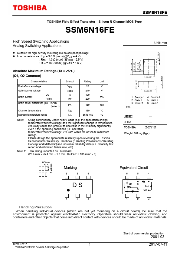
Unit: mm
JEDEC JEITA TOSHIBA
― ― 2-2N1D
Weight: 3.0 mg (typ.)
0.3 mm
0.45 mm
Marking
6
5
4
Equivalent Circuit
6
5
4
DS...