SPP1413
P-Channel Enhancement Mode MOSFET
DESCRIPTION The SPP1413 is the P-Channel logic enhancement mode power field e...
SPP1413
P-Channel Enhancement Mode
MOSFET
DESCRIPTION The SPP1413 is the P-Channel logic enhancement mode power field effect transistors are produced using high cell density , DMOS trench technology. This high density process is especially tailored to minimize on-state resistance. These devices are particularly suited for low
voltage application such as cellular phone and notebook computer power management and other battery powered circuits where high-side switching , and low in-line power loss are needed in a very small outline surface mount package.
APPLICATIONS Power Management in Note book Portable Equipment Battery Powered System DC/DC Converter Load Switch DSC LCD Display inverter
FEATURES -20V/-2.4A,RDS(ON)=130mΩ@VGS=-10V -20V/-2.9A,RDS(ON)=150mΩ@VGS=-4.5V Super high density cell design for extremely low
RDS (ON) Exceptional on-resistance and maximum DC
current capability SOT-323 ( SC–70 ) package design
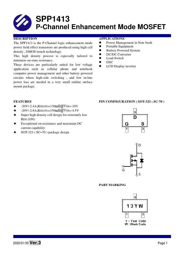
PIN CONFIGURATION ( SOT-323 ; SC-70 )
PART MARKING
2020/01/30 Ver.3
Page 1
SPP1413
P-Channel Enhancement Mode
MOSFET
PIN DESCRIPTION Pin 1 2 3
Symbol G S D
Description Gate Source Drain
ORDERING INFORMATION
Part Number
Package
SPP1413S32RGB
SOT-323
※ Week Code : A ~ Z( 1 ~ 26 ) ; a ~ z( 27 ~ 52 ) ※ SPP1413S32RGB : Tape Reel ; Pb – Free; Halogen - Free
Part Marking 13
ABSOULTE MAXIMUM RATINGS (TA=25℃ Unless otherwise noted)
Parameter
Drain-Source
Voltage
Gate –Source
Voltage Continuous Drain Current(TJ=150℃) Pulsed Drain Curre...