SPN2324
N-Channel Enhancement Mode MOSFET
DESCRIPTION The SPN2324 is the N-Channel logic enhancement mode power field e...
SPN2324
N-Channel Enhancement Mode
MOSFET
DESCRIPTION The SPN2324 is the N-Channel logic enhancement mode power field effect transistor which is produced using super high cell density DMOS trench technology. The SPN2324 has been designed specifically to improve the overall efficiency of DC/DC converters using either synchronous or conventional switching PWM controllers. It has been optimized for low gate charge, low RDS(ON) and fast switching speed.
APPLICATIONS Powered System DC/DC Converter Load Switch
FEATURES 100V/3A,RDS(ON)=310mΩ@VGS=10V 100V/1.3A,RDS(ON)=330mΩ@VGS=4.5V High density cell design for extremely low RDS (ON) Exceptional on-resistance and maximum DC current
capability SOT-23 package design
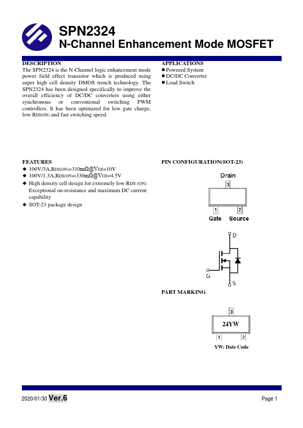
PIN CONFIGURATION(SOT-23)
2020/01/30 Ver.6
PART MARKING 24YW
YW: Date Code
Page 1
SPN2324
N-Channel Enhancement Mode
MOSFET
PIN DESCRIPTION Pin 1 2 3
Symbol G S D
Description Gate Source Drain
ORDERING INFORMATION
Part Number
Package
SPN2324S23RGB
SOT-23
※ SPN2324S23RGB : Tape Reel ; Pb – Free ; Halogen – Free
Part Marking 24
ABSOULTE MAXIMUM RATINGS (TA=25℃ Unless otherwise noted)
Parameter
Symbol
Drain-Source
Voltage
VDSS
Gate –Source
Voltage Continuous Drain Current(TJ=150℃) Pulsed Drain Current Power Dissipation Operating Junction Temperature Storage Temperature Range Thermal Resistance-Junction to Ambient
TA=25℃ TA=70℃
TA=25℃ TA=70℃
VGSS ID IDM PD TJ
TSTG RθJA
Typical 100
±30 3.0 2.0 10 1.25 0.8 -55/150 -55/150 100
Unit V V
A
...