SPD50N03S2L-06 OptiMOS® Power-Transistor
Feature
• N-Channel
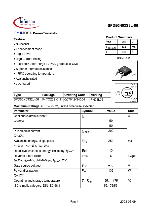
Product Summary VDS R DS(on) ID 30 6.4 50
P- TO252 -3-11
...
SPD50N03S2L-06 OptiMOS® Power-Transistor
Feature
N-Channel
Product Summary VDS R DS(on) ID 30 6.4 50
P- TO252 -3-11
V mΩ A
Enhancement mode Logic Level High Current Rating Excellent Gate Charge x R DS(on) product (FOM)
Superior thermal resistance
175°C operating temperature Avalanche rated dv/dt rated
Type SPD50N03S2L-06
Package Ordering Code P- TO252 -3-11 Q67042-S4084
Marking PN03L06
Maximum Ratings, at Tj = 25 °C, unless otherwise specified Parameter Continuous drain current1)
TC=25°C
Symbol ID
Value 50 50
Unit A
Pulsed drain current
TC=25°C
ID puls EAS EAR dv/dt VGS Ptot T j , Tstg
200 250 13 6 ±20 136 -55... +175 55/175/56 kV/µs V W °C mJ
Avalanche energy, single pulse
ID=50 A , V DD=25V, RGS=25Ω
Repetitive avalanche energy, limited by Tjmax 2) Reverse diode d v/dt
IS=50A, VDS=24V, di/dt=200A/µs, T jmax=175°C
Gate source
voltage Power dissipation
TC=25°C
Operating and storage temperature IEC climatic category; DIN IEC 68-1
Page 1
2003-05-09
SPD50N03S2L-06
Thermal Characteristics Parameter Characteristics Thermal resistance, junction - case Thermal resistance, junction - ambient, leaded SMD version, device on PCB:
@ min. footprint @ 6 cm2 cooling area
3)
Symbol min. RthJC RthJA RthJA -
Values typ. 0.7 max. 1.1 100 75 50
Unit
K/W
Electrical Characteristics, at Tj = 25 °C, unless otherwise specified Parameter Static Characteristics Drain-source breakdown
voltage
V GS=0V, ID=1mA
Symbol min. V(BR)DSS VGS(th) IDSS IGSS RDS(on) RDS(o...