SPD31N05 SPU31N05
SIPMOS ® Power Transistor
• N channel • Enhancement mode • Avalanche-rated • dv /dt rated • 175°C op...
SPD31N05 SPU31N05
SIPMOS ® Power Transistor
N channel Enhancement mode Avalanche-rated dv /dt rated 175°C operating temperature
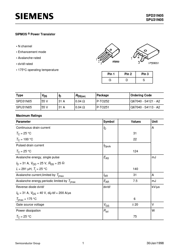
Pin 1 Pin 2 Pin 3
G
D
S
Type
VDS 55 V 55 V
ID 31 A 31 A
RDS(on) 0.04 Ω 0.04 Ω
Package
Ordering Code
SPD31N05 SPU31N05
P-TO252 P-TO251
Q67040 - S4121 - A2 Q67040 - S4113 - A2
Maximum Ratings Parameter Symbol Values Unit
Continuous drain current
TC = 25 °C TC = 100 °C
ID
A 31 22
Pulsed drain current
TC = 25 °C
IDpuls
124
EAS
Avalanche energy, single pulse
ID = 31 A, V DD = 25 V, RGS = 25 Ω L = 291 µH, Tj = 25 °C
mJ
140
IAR EAR
Avalanche current,limited by Tjmax Avalanche energy,periodic limited by Tjmax Reverse diode dv/dt
IS = 31 A, VDS = 40 V, diF/dt = 200 A/µs Tjmax = 175 °C
31 7.5
A mJ kV/µs
dv /dt
6
VGS Ptot
Gate source
voltage Power dissipation
TC = 25 °C
± 20
75
V W
Semiconductor Group
1
30/Jan/1998
SPD31N05 SPU31N05
Maximum Ratings Parameter Symbol Values Unit
Operating temperature Storage temperature Thermal resistance, junction - case Thermal resistance, junction - ambient (PCB mount)** Thermal resistance, junction - ambient IEC climatic category, DIN IEC 68-1
Tj Tstg RthJC RthJA RthJA
-55 ... + 175 -55 ... + 175
°C
≤2 ≤ 50 ≤ 100
55 / 175 / 56
K/W
** when mounted on 1 " square PCB ( FR4 );for recommended footprint
Electrical Characteristics, at Tj = 25°C, unless otherwise specified Parameter Symbol min. Static Characteristics Values typ. max. Unit
Drain- source breakdown
voltage
V GS = 0...