Preliminary Data
SIPMOS® Power Transistor
Features • N channel
•
SPD 10N10
Product Summary Drain source voltage Drain...
Preliminary Data
SIPMOS® Power Transistor
Features N channel
SPD 10N10
Product Summary Drain source
voltage Drain-Source on-state resistance Continuous drain current
VDS RDS(on) ID
100 0.2 10
V Ω A
Enhancement mode
Avalanche rated dv/dt rated
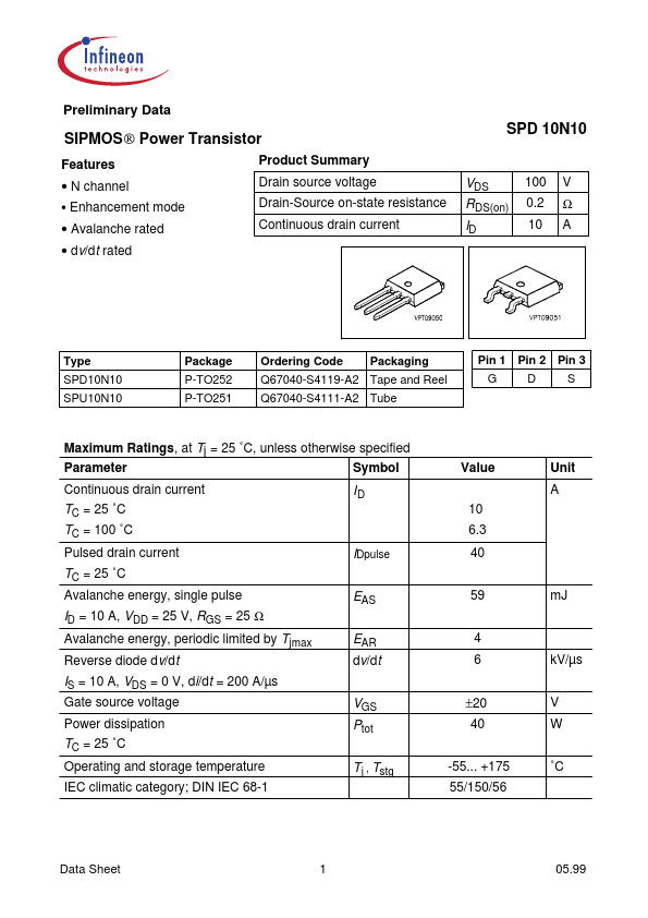
Type SPD10N10 SPU10N10
Package P-TO252 P-TO251
Ordering Code
Packaging
Pin 1 G
Pin 2 Pin 3 D S
Q67040-S4119-A2 Tape and Reel Q67040-S4111-A2 Tube
Maximum Ratings, at Tj = 25 ˚C, unless otherwise specified Parameter Continuous drain current Symbol Value 10 6.3 40 59 4 6 ±20 40 -55... +175 55/150/56 kV/µs V W ˚C mJ Unit A
ID
TC = 25 ˚C TC = 100 ˚C
Pulsed drain current
IDpulse EAS EAR
dv/dt
TC = 25 ˚C
Avalanche energy, single pulse
ID = 10 A, VDD = 25 V, RGS = 25 Ω
Avalanche energy, periodic limited by Tjmax Reverse diode dv/dt
IS = 10 A, VDS = 0 V, di/dt = 200 A/µs
Gate source
voltage Power dissipation
VGS Ptot T j , Tstg
TC = 25 ˚C
Operating and storage temperature IEC climatic category; DIN IEC 68-1
Data Sheet
1
05.99
SPD 10N10
Thermal Characteristics Parameter Characteristics Thermal resistance, junction - case Thermal resistance, junction - ambient, leded SMD version, device on PCB: @ min. footprint @ 6 cm 2 cooling area1) Symbol min. Values typ. max. 3.1 100 75 50 K/W Unit
RthJC RthJA RthJA
-
Electrical Characteristics , at Tj = 25 ˚C, unless otherwise specified Parameter Static Characteristics Drain- source breakdown
voltage Symbol min. Values typ. 3 max. 4 µA 0.1 10 1 100 100 nA Ω 0.15 0.2 V U...