Preliminary data
SPD02N60 SPU02N60
SIPMOS® Power Transistor • N-Channel
• Enhancement mode
• Avalanche rated
www.Data...
Preliminary data
SPD02N60 SPU02N60
SIPMOS® Power Transistor N-Channel
Enhancement mode
Avalanche rated
www.DataSheet4U.com
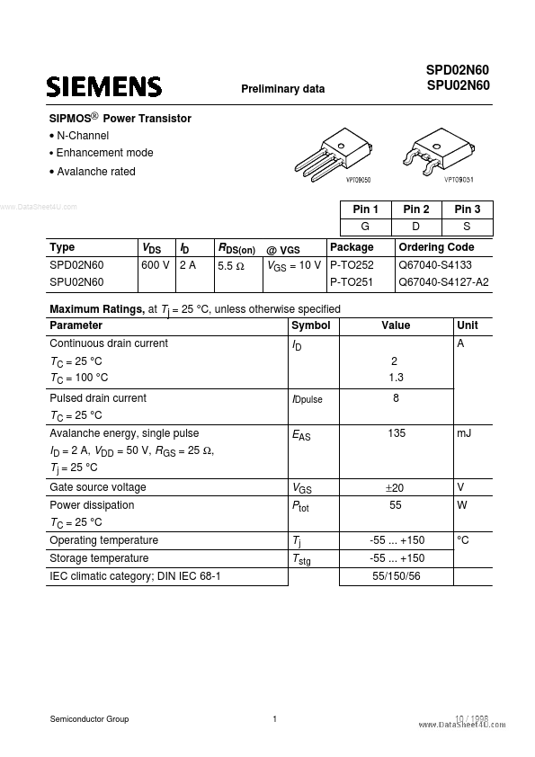
Pin 1 G
Pin 2 D
Pin 3 S
Type SPD02N60 SPU02N60
VDS
ID
600 V 2 A
RDS(on) @ VGS Package VGS = 10 V P-TO252 5.5 Ω P-TO251
Ordering Code Q67040-S4133 Q67040-S4127-A2
Maximum Ratings, at T j = 25 °C, unless otherwise specified Symbol Parameter Continuous drain current
Value 2 1.3 8 135
Unit A
ID
T C = 25 °C T C = 100 °C
Pulsed drain current
IDpulse EAS
T C = 25 °C
Avalanche energy, single pulse mJ
I D = 2 A, VDD = 50 V, R GS = 25 Ω, T j = 25 °C
Gate source
voltage Power dissipation
VGS Ptot Tj T stg
±20 55 -55 ... +150 -55 ... +150 55/150/56
V W °C
T C = 25 °C
Operating temperature Storage temperature IEC climatic category; DIN IEC 68-1
Semiconductor Group
1
10 / 1998
Preliminary data
SPD02N60 SPU02N60
Electrical Characteristics Parameter at Tj = 25 °C, unless otherwise specified Thermal Characteristics Thermal resistance, junction - case
www.DataSheet4U.com
Symbol min.
Values typ. max. 2.25 100 50 tbd -
Unit
RthJC RthJA RthJA
-
K/W
Thermal resistance, junction - ambient SMD version, device on PCB: @ min. footprint @ 6 cm 2 cooling area1)
Static Characteristics Drain- source breakdown
voltage
V(BR)DSS VGS(th) I DSS
600 2.1
3
4
V
VGS = 0 V, I D = 0.25 mA
Gate threshold
voltage, VGS = VDS I D = 1 mA Zero gate
voltage drain current
µA 0.1 10 4.2 1 100 100 5.5 nA Ω
VDS = 600 V, VGS = 0 V, T j = 25 °C VDS = 600 V,...