SPI80N04S2-04 SPP80N04S2-04,SPB80N04S2-04
OptiMOS Power-Transistor
Feature
• N-Channel
Product Summary VDS RDS(on) ma...
SPI80N04S2-04 SPP80N04S2-04,SPB80N04S2-04
OptiMOS Power-Transistor
Feature
N-Channel
Product Summary VDS RDS(on) max. SMD version ID
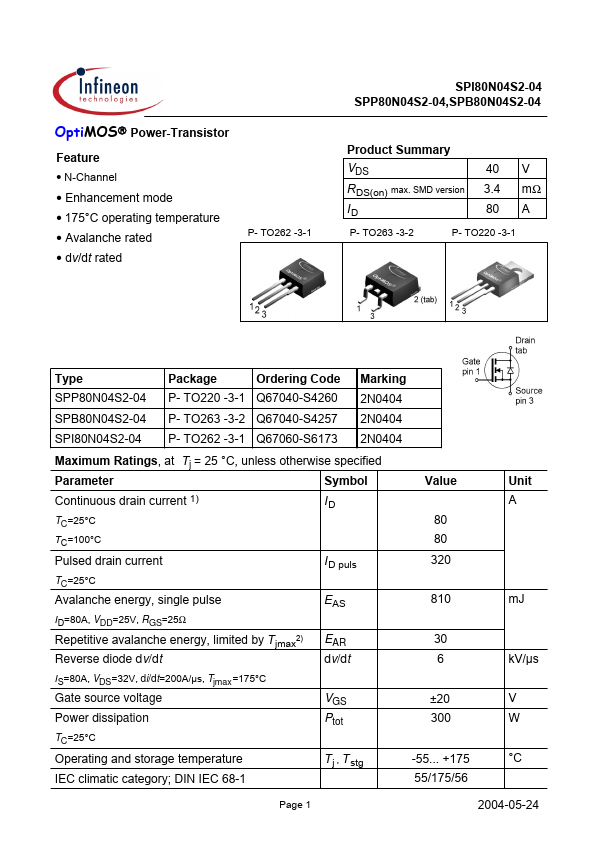
P- TO262 -3-1 P- TO263 -3-2
40 3.4 80
P- TO220 -3-1
V mΩ A
Enhancement mode 175°C operating temperature Avalanche rated dv/dt rated
Type SPP80N04S2-04 SPB80N04S2-04 SPI80N04S2-04
Package
Ordering Code
Marking 2N0404 2N0404 2N0404 Value 80 80 Unit A
P- TO220 -3-1 Q67040-S4260 P- TO263 -3-2 Q67040-S4257 P- TO262 -3-1 Q67060-S6173
Maximum Ratings, at Tj = 25 °C, unless otherwise specified Symbol Parameter Continuous drain current 1)
TC=25°C TC=100°C
ID
Pulsed drain current
TC=25°C
I D puls EAS EAR dv/dt VGS Ptot T j , T stg
320 810 30 6 ±20 300 -55... +175 55/175/56 kV/µs V W °C mJ
Avalanche energy, single pulse
ID=80A, VDD=25V, RGS=25Ω
Repetitive avalanche energy, limited by Tjmax2)
Reverse diode dv/dt
IS=80A, VDS=32V, di/dt=200A/µs, Tjmax =175°C
Gate source
voltage Power dissipation
TC=25°C
Operating and storage temperature IEC climatic category; DIN IEC 68-1
Page 1
2004-05-24
SPI80N04S2-04 SPP80N04S2-04,SPB80N04S2-04 Thermal Characteristics Parameter Characteristics Thermal resistance, junction - case Thermal resistance, junction - ambient, leaded SMD version, device on PCB:
@ min. footprint @ 6 cm2 cooling area 3)
Symbol min.
RthJC RthJA RthJA
Values typ. 0.3 max. 0.5 62 62 40
Unit
-
K/W
Electrical Characteristics, at Tj = 25 °C, unless otherwise specified Parameter Static Characteristics Drain-source break...