SN74HC08, SN54HC08
SCLS081I – DECEMBER 1982 – REVISED SEPTEMBER 2021
SNx4HC08 Quadruple 2-Input AND Gates
1 Features
• ...
SN74HC08, SN54HC08
SCLS081I – DECEMBER 1982 – REVISED SEPTEMBER 2021
SNx4HC08 Quadruple 2-Input AND Gates
1 Features
Buffered inputs Wide operating
voltage range: 2 V to 6 V Wide operating temperature range:
–40°C to +85°C Supports fanout up to 10 LSTTL loads Significant power reduction compared to LSTTL
logic ICs
2 Applications
Combining power good signals Enable digital signals
3 Description
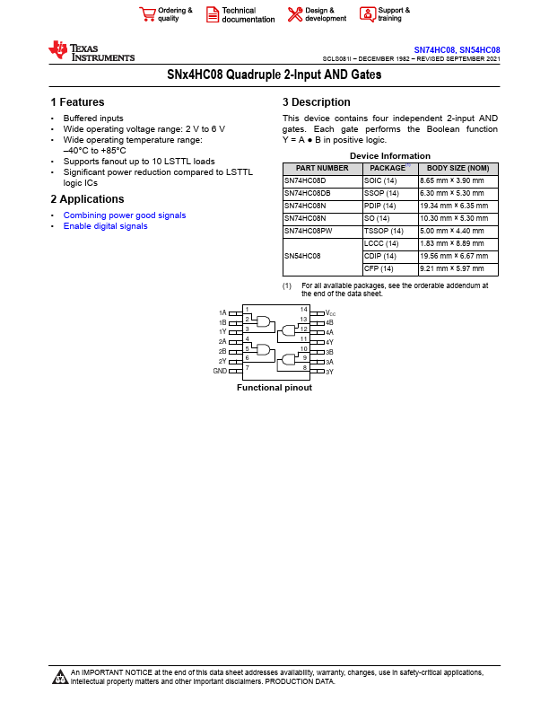
This device contains four independent 2-input AND gates. Each gate performs the Boolean function Y = A ● B in positive logic.
Device Information
PART NUMBER
PACKAGE(1)
BODY SIZE (NOM)
SN74HC08D
SOIC (14)
8.65 mm × 3.90 mm
SN74HC08DB
SSOP (14)
6.30 mm × 5.30 mm
SN74HC08N
PDIP (14)
19.34 mm × 6.35 mm
SN74HC08N
SO (14)
10.30 mm × 5.30 mm
SN74HC08PW
TSSOP (14) 5.00 mm × 4.40 mm
LCCC (14)
1.83 mm × 8.89 mm
SN54HC08
CDIP (14)
19.56 mm × 6.67 mm
CFP (14)
9.21 mm × 5.97 mm
(1) For all available packages, see the orderable addendum at the end of the data sheet.
1A
1
1B
2
1Y
3
2A
4
2B
5
2Y
6
GND
7
14
VCC
13 4B
12 4A
11 4Y
10 3B
9 3A
8 3Y
Functional pinout
An IMPORTANT NOTICE at the end of this data sheet addresses availability, warranty, changes, use in safety-critical applications, intellectual property matters and other important disclaimers. PRODUCTION DATA.
SN74HC08, SN54HC08
SCLS081I – DECEMBER 1982 – REVISED SEPTEMBER 2021
www.ti.com
Table of Contents
1 Features...............................................................