SLG8SP513
Clock Synthesizer for Intel Mobile PCI-Express Chipset
Features
• Low Power CK505 compatible clock synthesize...
SLG8SP513
Clock Synthesizer for Intel Mobile PCI-Express Chipset
Features
Low Power CK505 compatible clock synthesizer
SLG8SP513 is a cost reduced CK505 with integrated
voltage regulator for mobile applications
Scalable Low
Voltage VDD I/O (3.3V to 1.05V) to reduce power consumption
Low Power differential outputs with integrated series termination resistors (50 ohm resistor to GND and 33 ohm series resistor not needed)
Integrated CK_SSCD function to provide additional Spread Spectrum support for GMCH
CLK_REQ# inputs to support SRC clock power management
64 pin QFN Package
Output Summary
2- differential CPU clock outputs @ 0.7V 1 - selectable differential CPU/SRC clock output @ 0.7V 1 - selectable differential DOT96/SRC clock output @ 0.7V 8 - differential Serial Reference Clock (SRC) clock outputs
@ 0.7V 1 - selectable LCDCLK/27M clock output 1 - single-ended 48MHz clock output @ 3.3V 6 - single-ended 33MHz clock outputs @ 3.3V 1 - single-ended 14.318MHz clock output @ 3.3V
Table 1. Frequency Select Table (FS_C, FS_B, FS_A)
FFF SSS ___ CBA
000
001
010
011
100
101
110
111
CPU (MHz) 266.6 133.3 200.0 166.6 333.3 100.0 400.0
SRC (MHz) 100.0 100.0 100.0 100.0 100.0 100.0 100.0
PCI REF (MHz) (MHz) 33.3 14.318 33.3 14.318 33.3 14.318 33.3 14.318 33.3 14.318 33.3 14.318 33.3 14.318
Reserved
DOT_ 96
(MHz)
96.0
96.0
96.0
96.0
96.0
96.0
96.0
USB (MHz) 48.0 48.0 48.0 48.0 48.0 48.0 48.0
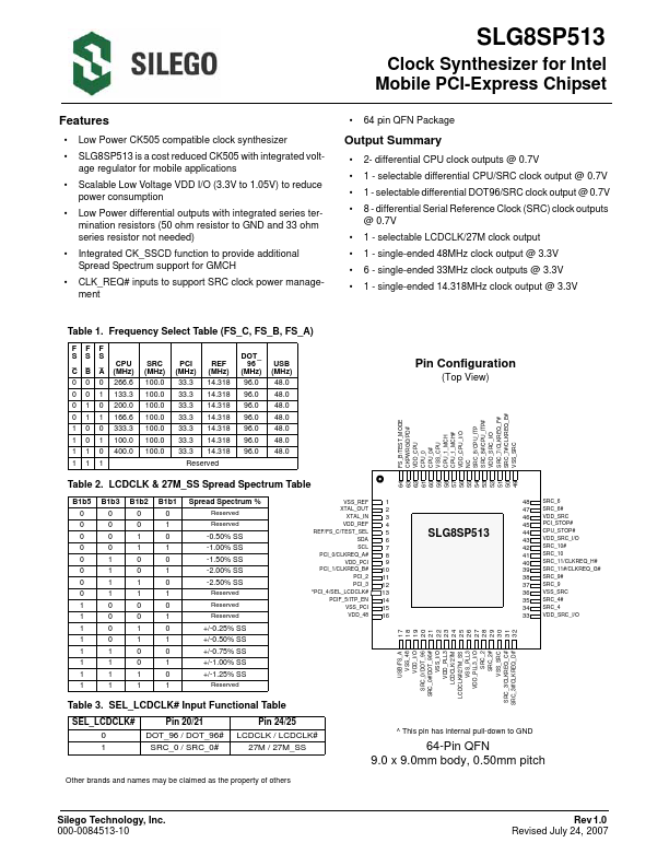
Pin Configuration
(Top View)
FS_B/TEST_MODE CKPWRGD/PD# VDD_...