SLC555
Timing Circuit
The SLC555 monolithic timing circuit is a highly stable controller capable of producing accurate ...
SLC555
Timing Circuit
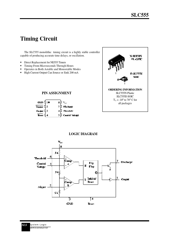
The SLC555 monolithic timing circuit is a highly stable controller capable of producing accurate time delays, or oscillation. Direct Replacement for NE555 Timers Timing From Microseconds Through Hours Operates in Both Astable and Monostable Modes High Current Output Can Source or Sink 200 mA
PIN ASSIGNMENT
ORDERING INFORMATION SLC555N Plastic SLC555D SOIC TA = -10° to 70° C for all packages
LOGIC DIAGRAM
SLS
System Logic Semiconductor
SLC555
MAXIMUM RATINGS *
Symbol VCC Tstg Supply
Voltage Storage Temperature Parameter Value 18 -60 to +85 Unit V °C
RECOMMENDED OPERATING CONDITIONS
Symbol VCC TA Supply
Voltage Operating Temperature, All Package Types Parameter Min 4.5 -10 Max 16 +70 Unit V °C
ELECTRICAL CHARACTERISTICS (TA =+25°C)
Symbol Parameter Test Conditions VCC=5.0 V, RL =∞ VCC=15 V, RL=∞ R=1.0 kΩ to 100 kΩ Initial Accuracy C = 0.1 µF VCC=5.0 V and VCC=15 V VCC=5.0 V VCC=15 V VCC=5.0 V VCC=15 V V02=0 V, VCC=15 V V02=15 V, VCC=15 V VCC=15 V V04=0 V, VCC=15 V V04=15 V, VCC=15 V V06=0 V, VCC=15 V V06=10 V, VCC=15 V 0.4 2.6 9 1.1 4.5 Guaranteed Limits Min ICC Supply Current Timing Error Max 6.0 15 4 mA % Unit
Vth VT IT VR IR Ith Idis VREF VOL
Threshold
Voltage Trigger
Voltage Trigger Current Reset
Voltage Reset Current Threshold Current (Note 1)
4.0 11 2.2 5.6 -2 0.5 1.0 -0.4 0.5 -0.5 0.25 100
V V µA V mA µA µA nA V V
Discharge Leakage Current (Pin VCC=15 V, V07=15 V 7) Control
Voltage Level Output
Voltage Low VCC=15 V VCC=5.0 V (V...