SLA5002
Absolute maximum ratings
Symbol VDSS VGSS ID ID(pulse) EAS* IF IFSM VR PT Ratings 100 ±20 ±5 ±10 (PW≤1ms) 30 5 (...
SLA5002
Absolute maximum ratings
Symbol VDSS VGSS ID ID(pulse) EAS* IF IFSM VR PT Ratings 100 ±20 ±5 ±10 (PW≤1ms) 30 5 (PW≤0.5ms, Du≤25%) 10 (PW≤10ms, Single Pulse) 120
N-channel With built-in flywheel diode
(Ta=25°C)
External dimensions A
SLA
Electrical characteristics
Symbol V(BR)DSS IGSS IDSS VTH Re(yfs) RDS(ON) Ciss Coss ton toff VSD trr Specification min typ max 100 ±500 250 2.0 4.0 2.4 3.7 0.27 0.30 350 130 60 40 1.1 1.8 330 Specification typ max 1.0 100 1.2 10 Unit V nA µA V S Ω pF pF ns ns V ns
(Ta=25°C)
Unit V V A A mJ A A V W W °C/W °C/W Vrms °C °C
Conditions ID=250µA, VGS=0V VGS=±20V VDS=100V, VGS=0V VDS=10V, ID=250µA VDS=10V, ID=5A VGS=10V, ID=5A VDS=25V, f=1.0MHz, VGS=0V ID=5A, VDD 50V,VGS=10V, see Fig. 3 on page 16. ISD=5A, VGS=0V ISD=±100mA
θ j-a θ j-c VISO Tch Tstg
5 (Ta=25°C, with all circuits operating, without heatsink) 35 (Tc=25°C,with all circuits operating, with infinite heatsink) 25 (Junction-Air, Ta=25°C, with all circuits operating) 3.57 (Junction-Case, Tc=25°C, with all circuits operating) 1000 (Between fin and lead pin, AC) 150 –40 to +150
qDiode for flyback
voltage absorption
Symbol VR VF IR trr min 120 Unit V V µA ns Conditions IR=10µA IF=1A VR=120V IF=±100mA
* : VDD=20V, L=10mH, ID=2.5A, unclamped, see Fig. E on page 15
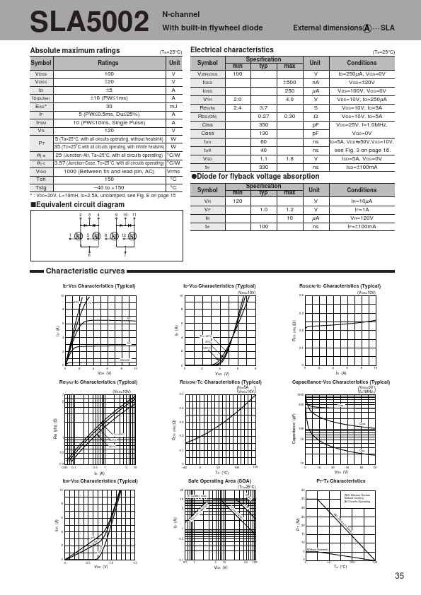
sEquivalent circuit diagram
2 3 4 9 10 11
1
5
8
12
6
7
Characteristic curves
ID-VDS Characteristics (Typical)
10
10V 7V
ID-VGS Characteristics (Typical)
(VDS=10V)
10
RDS(ON)-ID Characteristics (Typical)
0...