Si9926BDY
Vishay Siliconix
Dual N-Channel 2.5-V (G-S) MOSFET
PRODUCT SUMMARY
VDS (V)
RDS(on) (Ω)
20 0.020 at VGS = 4...
Si9926BDY
Vishay Siliconix
Dual N-Channel 2.5-V (G-S)
MOSFET
PRODUCT SUMMARY
VDS (V)
RDS(on) (Ω)
20 0.020 at VGS = 4.5 V 0.030 at VGS = 2.5 V
ID (A) 8.2 6.7
FEATURES
Halogen-free According to IEC 61249-2-21 Definition
TrenchFET® Power
MOSFETS Compliant to RoHS Directive 2002/95/EC
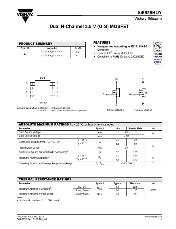
S1 1 G1 2 S2 3 G2 4
SO-8
8 D1 7 D1 6 D2 5 D2
Top View
Ordering Information: Si9926BDY-T1-E3 (Lead (Pb)-free) Si9926BDY-T1-GE3 (Lead (Pb)-free and Halogen-free)
D1 D2
G1 G2
S1 N-Channel
MOSFET
S2 N-Channel
MOSFET
ABSOLUTE MAXIMUM RATINGS TA = 25 °C, unless otherwise noted
Parameter
Symbol
10 s
Steady State
Drain-Source
Voltage
VDS 20
Gate-Source
Voltage
VGS
± 12
Continuous Drain Current (TJ = 150 °C)a
TA = 25 °C TA = 70 °C
ID
8.2 6.2 6.5 4.9
Pulsed Drain Current
IDM 30
Continuous Source Current (Diode Conduction)a
IS 1.7 0.95
Maximum Power Dissipationa
TA = 25 °C TA = 70 °C
PD
2.0 1.14 1.3 0.72
Operating Junction and Storage Temperature Range
TJ, Tstg
- 55 to 150
Unit V
A
W °C
THERMAL RESISTANCE RATINGS
Parameter
Maximum Junction-to-Ambienta
Maximum Junction-to-Foot (Drain) Notes: a. Surface Mounted on 1" x 1" FR4 board.
t ≤ 10 s Steady State Steady State
Symbol RthJA RthJF
Typical 52 90 32
Maximum 62.5 110 40
Unit °C/W
Document Number: 72278 S09-0870-Rev. C, 18-May-09
www.vishay.com 1
Si9926BDY
Vishay Siliconix
SPECIFICATIONS TJ = 25 °C, unless otherwise noted
Parameter
Symbol
Test Conditions
Static
Gate Threshold
Voltage
VGS(th)
VDS = V...