Si5853DC
Vishay Siliconix
P-Channel 1.8 V (G-S) MOSFET with Schottky Diode
MOSFET PRODUCT SUMMARY
VDS (V)
RDS(on) (Ω)...
Si5853DC
Vishay Siliconix
P-Channel 1.8 V (G-S)
MOSFET with Schottky Diode
MOSFET PRODUCT SUMMARY
VDS (V)
RDS(on) (Ω)
0.110 at VGS = - 4.5 V - 20 0.160 at VGS = - 2.5 V
0.240 at VGS = - 1.8 V
ID (A) - 3.6 - 3.0 - 2.4
SCHOTTKY PRODUCT SUMMARY
VKA (V) 20
Vf (V) Diode Forward
Voltage
0.48 V at 0.5 A
IF (A) 1.0
FEATURES
Halogen-free According to IEC 61249-2-21 Definition
LITTLE FOOT® Plus
Compliant to RoHS Directive 2002/95/EC
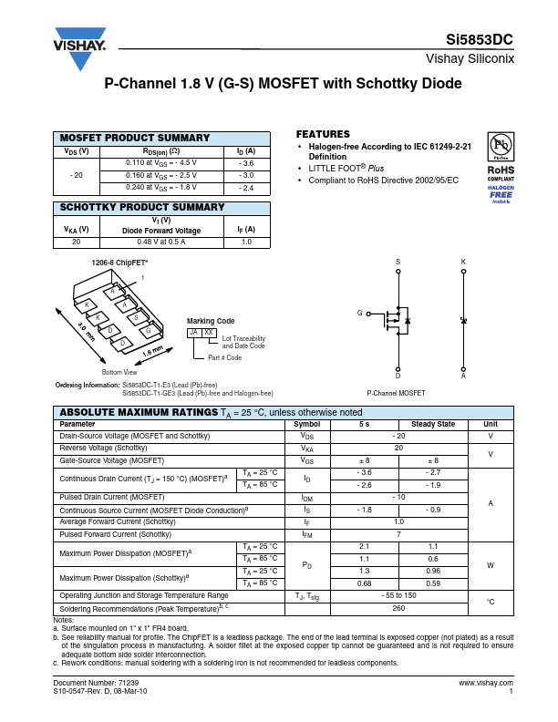
1206-8 ChipFET®
1
A
K K
A S
DG
D
Marking Code
JA XX Lot Traceability and Date Code
Part # Code
Bottom View
Ordering Information: Si5853DC-T1-E3 (Lead (Pb)-free) Si5853DC-T1-GE3 (Lead (Pb)-free and Halogen-free)
S G
K
D P-Channel
MOSFET
A
ABSOLUTE MAXIMUM RATINGS TA = 25 °C, unless otherwise noted
Parameter
Symbol
5s
Steady State
Unit
Drain-Source
Voltage (
MOSFET and Schottky)
VDS - 20
V
Reverse
Voltage (Schottky) Gate-Source
Voltage (
MOSFET)
VKA VGS
20 ±8 ±8
V
Continuous Drain Current (TJ = 150 °C) (
MOSFET)a
TA = 25 °C TA = 85 °C
ID
- 3.6 - 2.6
- 2.7 - 1.9
Pulsed Drain Current (
MOSFET) Continuous Source Current (
MOSFET Diode Conduction)a
IDM - 10
IS - 1.8
- 0.9
A
Average Forward Current (Schottky)
IF 1.0
Pulsed Forward Current (Schottky)
IFM 7
Maximum Power Dissipation (
MOSFET)a Maximum Power Dissipation (Schottky)a
TA = 25 °C TA = 85 °C TA = 25 °C TA = 85 °C
PD
2.1 1.1 1.3 0.68
1.1 0.6
W 0.96 0.59
Operating Junction and Storage Temperature Range Soldering Recommendations (Peak Temperature)b, c
...