SEMD4
NPN/PNP Silicon Digital Transistor Array Preliminary data • Switching circuit, inverter, interface circuit, driver...
SEMD4
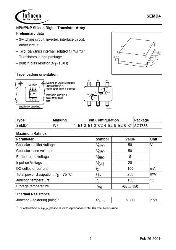
NPN/PNP Silicon Digital Transistor Array Preliminary data Switching circuit, inverter, interface circuit, driver circuit Two (galvanic) internal isolated NPN/PNP Transistors in one package Built in bias resistor (R1=10kΩ) Tape loading orientation
Top View
3 2 1
4 5 3 6 1 2
Marking on SOT666 package (for example W R) corresponds to pin 1 of device Position in tape: pin 1 same of feed hole side
C1 6
B2 5
E2 4
R2 R1 TR1 R2 1 2 B1 3 C2
EHA07176
TR2 R1
4 5 6
Direction of Unreeling
Type SEMD4
Maximum Ratings Parameter
Collector-emitter
voltage Collector-base
voltage Emitter-base
voltage Input on
Voltage DC collector current Total power dissipation, TS = 75 °C Junction temperature Storage temperature
Thermal Resistance
Junction - soldering point 1)
1For calculation of R thJA please refer to Application Note Thermal Resistance
WR
E1
Marking W7
Pin Configuration Package 1=E1 2=B1 3=C2 4=E2 5=B2 6=C1 SOT666
Symbol VCEO VCBO VEBO Vi(on) IC Ptot Tj Tstg
Value 50 50 5 20 100 250 150 -65 ... 150
Unit V
mA mW °C
RthJS
≤ 300
K/W
1
Feb-26-2004
SEMD4
Electrical Characteristics at TA=25°C, unless otherwise specified Parameter Symbol Values min. DC Characteristics Collector-emitter breakdown
voltage IC = 100 µA, IB = 0 Collector-base breakdown
voltage IC = 10 µA, IE = 0 Collector cutoff current VCB = 40 V, IE = 0 DC current gain 1) IC = 5 mA, VCE = 5 V Collector-emitter saturation
voltage1) IC = 10 mA, IB = 0.5 mA Input off
voltage IC = 100 µA, VCE = 5 V I...