SEMB11
PNP Silicon Digital Transistor Array Preliminary data • Switching circuit, inverter, interface circuit, driver ci...
SEMB11
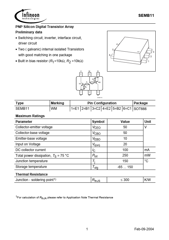
PNP Silicon Digital Transistor Array Preliminary data Switching circuit, inverter, interface circuit, driver circuit Two ( galvanic) internal isolated Transistors with good matching in one package Built in bias resistor ( R1 =10kΩ, R2 =10kΩ)
C1 6 B2 5 E2 4
4 5 3 6 1 2
R2 R1 TR1 R2 1 E1 2 B1 3 C2
EHA07173
TR2 R1
Type SEMB11
Maximum Ratings Parameter
Marking WM
Pin Configuration Package 1=E1 2=B1 3=C2 4=E2 5=B2 6=C1 SOT666
Symbol VCEO VCBO VEBO Vi(on) IC Ptot Tj T stg
Value
Unit
Collector-emitter
voltage Collector-base
voltage Emitter-base
voltage Input on
Voltage DC collector current Total power dissipation , TS = 75 °C Junction temperature Storage temperature Thermal Resistance
50 50 10 20 100 250 150 -65 ... 150
V
mA mW °C
Junction - soldering point1)
RthJS
≤ 300
K/W
1For calculation of R thJA please refer to Application Note Thermal Resistance
1
Feb-09-2004
SEMB11
Electrical Characteristics at TA=25°C, unless otherwise specified Parameter Symbol Values min. DC Characteristics Collector-emitter breakdown
voltage IC = 100 µA, IB = 0 Collector-base breakdown
voltage IC = 10 µA, IE = 0 Collector cutoff current VCB = 40 V, IE = 0 Emitter cutoff current VEB = 10 V, IC = 0 DC current gain 1) IC = 5 mA, VCE = 5 V Collector-emitter saturation
voltage1) IC = 10 mA, IB = 0.5 mA Input off
voltage IC = 100 µA, VCE = 5 V Input on
Voltage IC = 2 mA, VCE = 0.3 V Input resistor Resistor ratio R1 R1/R2 7 0.9 10 1 13 1.1 Vi(on) 1 2.5 Vi(off) 0.8 1.5 VCEsat 0...