SCH1337
Power MOSFET –30V, 150mΩ, –2A, Single P-Channel
This Low-profile High-power MOSFET is produced using ON Semicon...
SCH1337
Power
MOSFET –30V, 150mΩ, –2A, Single P-Channel
This Low-profile High-power
MOSFET is produced using ON Semiconductor’s trench technology, which is specifically designed to minimize gate charge and ultra low on resistance. This device is suitable for applications with low gate charge driving or ultra low on resistance requirements.
Features Low On-Resistance 4V drive Pb-Free, Halogen Free and RoHS compliance Ultra small package SCH6 (1.6mm×1.6mm×0.56mmt)
Typical Applications LCD Driver Load Switch
Voltage Protection
SPECIFICATIONS ABSOLUTE MAXIMUM RATING at Ta = 25°C (Note 1)
Parameter
Symbol
Value
Unit
Drain to Source
Voltage
VDSS
−30 V
Gate to Source
Voltage
VGSS
±20 V
Drain Current (DC)
ID −2 A
Drain Current (Pulse) PW ≤ 10μs, duty cycle ≤ 1%
IDP
−8 A
Power Dissipation
When mounted on ceramic substrate (900mm2 × 0.8mm)
PD
0.8 W
Junction Temperature
Tj 150 °C
Storage Temperature
Tstg
−55 to +150
°C
Note 1 : Stresses exceeding those listed in the Maximum Ratings table may damage
the device. If any of these limits are exceeded, device functionality should not
be assumed, damage may occur and reliability may be affected.
2 : This product is designed to “ESD immunity<200V*”, so please take care when
handling.
*Machine Model
THERMAL RESISTANCE RATINGS
Parameter
Junction to Ambient When mounted on ceramic substrate (900mm2 × 0.8mm)
Symbol RθJA
Value
Unit
156.2 °C/W
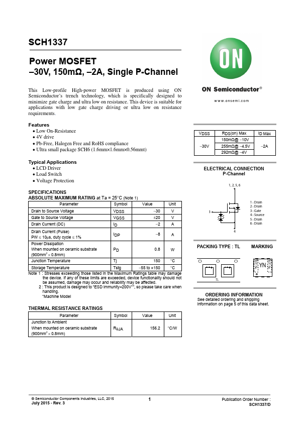
www.onsemi.com
VDSS −30V
RDS(on) Max 150mΩ@ −10V 255m...