Si1013R/X
New Product
Vishay Siliconix
P-Channel 1.8-V (G-S) MOSFET
PRODUCT SUMMARY
VDS (V) rDS(on) (W)
1.2 @ VGS = –4...
Si1013R/X
New Product
Vishay Siliconix
P-Channel 1.8-V (G-S)
MOSFET
PRODUCT SUMMARY
VDS (V) rDS(on) (W)
1.2 @ VGS = –4.5 V –20 1.6 @ VGS = –2.5 V 2.7 @ VGS = –1.8 V
ID (mA)
–350 –300 –150
FEATURES
D D D D D D High-Side Switching Low On-Resistance: 1.2 W Low Threshold: 0.8 V (typ) Fast Swtiching Speed: 14 ns 1.8-V Operation Gate-Source ESD Protection
BENEFITS
D D D D D Ease in Driving Switches Low Offset (Error)
Voltage Low-
Voltage Operation High-Speed Circuits Low Battery
Voltage Operation
APPLICATIONS
D Drivers: Relays, Solenoids, Lamps, Hammers, Displays, Memories D Battery Operated Systems D Power Supply Converter Circuits D Load/Power Switching Cell Phones, Pagers
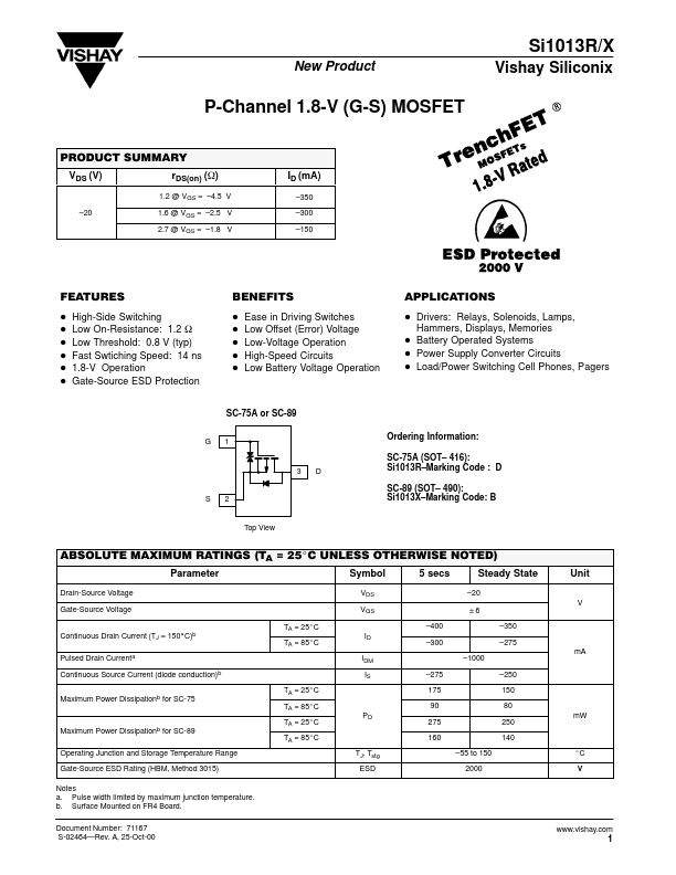
SC-75A or SC-89
G 1
Ordering Information: SC-75A (SOT– 416): Si1013R–Marking Code : D SC-89 (SOT– 490): Si1013X–Marking Code: B
Top View
3
D
S
2
ABSOLUTE MAXIMUM RATINGS (TA = 25_C UNLESS OTHERWISE NOTED)
Parameter
Drain-Source
Voltage Gate-Source
Voltage Continuous Drain Current (TJ = 150_C)b Pulsed Drain Currenta Continuous Source Current (diode conduction)b Maximum Power Dissipationb for SC-75 TA = 25_C TA = 85_C TA = 25_C for SC-89 TA = 85_C TJ, Tstg ESD PD TA = 25_C TA = 85_C ID IDM IS –275 175 90 275 160 –55 to 150 2000
Symbol
VDS VGS
5 secs
Steady State
–20 "6
Unit
V
–400 –300 –1000
–350 –275 mA –250 150 80 250 140 _C V mW
Maximum Power
Dissipationb
Operating Junction and Storage Temperature Range Gate-Source ESD Rating (HBM, Method 3015) Notes a. Pulse width limited by maximum junct...