Semiconductor
S358
Low Power Dual OP AMP
Description
The S358 consists of two independent high gain Internally frequen...
Semiconductor
S358
Low Power Dual OP AMP
Description
The S358 consists of two independent high gain Internally frequency compensated operational
amplifiers designed to operate from a single power supply over a wide range of
voltage.
Features
Input common mode
voltage range includes ground Internally frequency compensated for unity gain Large DC
voltage gain : 100dB Wide bandwidth for unity gain : 1 MHz Very low power consumption Wide supply
voltage range : Single : 3V ~ 30V, Dual : ±1.5 ~ ±15V
Applications
Transducer amplifier DC gain blocks Conventional operational
amplifiers
Ordering Information
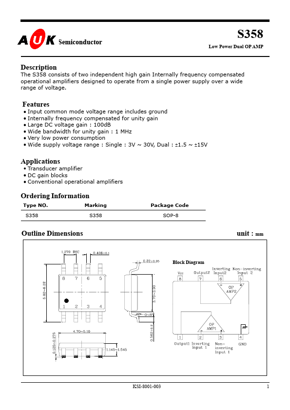
Type NO. S358 Marking S358 Package Code SOP-8
Outline Dimensions
unit : mm
Block Diagram
KSI-8001-003
1
S358
Absolute maximum ratings
Characteristic
Supply
voltage Differential input
voltage Input
voltage Power Dissipation Operating temperature Storage temperature
Symbol
VCC VIND VIN PD Topr Tstg
Ratings
36 or ±18 32 -0.3 ~ +32 300 -45 ~ +85 -55 ~ 150
Unit
V V V mW
°C °C
Electrical Characteristics
(Unless otherwise specified. VCC = 5V and –45 °C ≤ Ta ≤ +85 °C)
Characteristic
Input offset
voltage Input offset
voltage drift Input offset current Input offset current drift Input bias current
Symbol
VIOS ∆VIOS/∆T IIOS ∆IIOS/∆T IIB
Test Condition
5V ≤ VCC ≤ 30V Rg = 0Ω (Ta=25 °C) (Ta=25 °C) (Ta=25 °C) Rg = 0Ω, 0V ≤ VIC ≤ VCC-1.5V
Min. Typ. Max.
10 45 40 1 0.7 100 28 3 90 100 40 20 20 8 50 40 ±2 7 ±7 ±9 -
Unit
mV µV/ °C nA pA/ °C nA V V mA
±5
±50 ±15...