NPN/PNP Silicon Digital Tansistor Array (Switching circuit/ inverter/ interface circuit/ drive circuit)
BCR 22PN
NPN/PNP Silicon Digital Tansistor Array • Switching circuit, inverter, interface circuit, drive circuit • Two (...
BCR 22PN
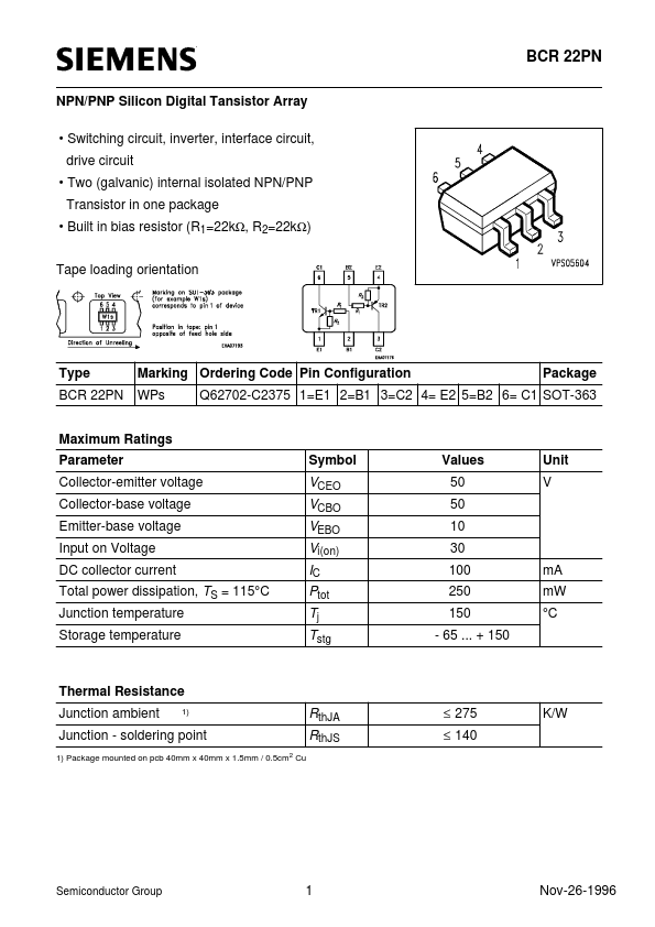
NPN/PNP Silicon Digital Tansistor Array Switching circuit, inverter, interface circuit, drive circuit Two (galvanic) internal isolated NPN/PNP Transistor in one package Built in bias resistor (R1=22kΩ, R2=22kΩ) Tape loading orientation
Type BCR 22PN
Marking Ordering Code Pin Configuration WPs
Package
Q62702-C2375 1=E1 2=B1 3=C2 4= E2 5=B2 6= C1 SOT-363
Maximum Ratings Parameter Collector-emitter
voltage Collector-base
voltage Emitter-base
voltage Input on
Voltage DC collector current Total power dissipation, TS = 115°C Junction temperature Storage temperature Symbol Values 50 50 10 30 100 250 150 - 65 ... + 150 mA mW °C Unit V
VCEO VCBO VEBO Vi(on) IC Ptot Tj Tstg
Thermal Resistance Junction ambient
1)
RthJA RthJS
≤ 275 ≤ 140
K/W
Junction - soldering point
1) Package mounted on pcb 40mm x 40mm x 1.5mm / 0.5cm2 Cu
Semiconductor Group
1
Nov-26-1996
BCR 22PN
Electrical Characteristics at TA=25°C, unless otherwise specified Parameter Symbol min. DC Characteristics Collector-emitter breakdown
voltage Values typ. max. Unit
V(BR)CEO
50 22 1 -
V
IC = 100 µA, IB = 0
Collector-base breakdown
voltage
V(BR)CBO
50
IC = 10 µA, IB = 0
Collector cutoff current
ICBO
100
nA µA 350 50 mV 0.3 V 0.8 1.5 2.5 29 1.1 kΩ -
VCB = 40 V, IE = 0
Emitter cutoff current
IEBO hFE VCEsat Vi(off) Vi(on)
1
VEB = 10 V, IC = 0
DC current gain
IC = 5 mA, VCE = 5 V
Collector-emitter saturation
voltage 1)
IC = 10 mA, IB = 0.5 mA
Input off
voltage
IC = 100 µA, VCE = 5 V
In...