Philips Semiconductors
Objective specification
TrenchMOS™ transistor
PSMN009-100W
FEATURES
• ’Trench’ technology • V...
Philips Semiconductors
Objective specification
TrenchMOS™ transistor
PSMN009-100W
FEATURES
’Trench’ technology Very low on-state resistance Fast switching High thermal cycling performance Low thermal resistance
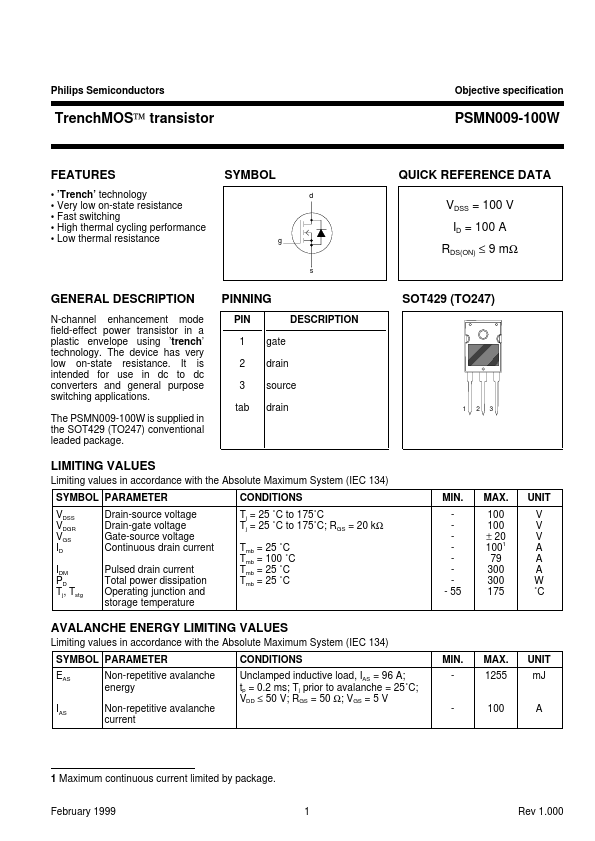
SYMBOL
d
QUICK REFERENCE DATA VDSS = 100 V ID = 100 A
g
RDS(ON) ≤ 9 mΩ
s
GENERAL DESCRIPTION
N-channel enhancement mode field-effect power transistor in a plastic envelope using ’trench’ technology. The device has very low on-state resistance. It is intended for use in dc to dc converters and general purpose switching applications. The PSMN009-100W is supplied in the SOT429 (TO247) conventional leaded package.
PINNING
PIN 1 2 3 tab gate drain source drain DESCRIPTION
SOT429 (TO247)
1
2
3
LIMITING VALUES
Limiting values in accordance with the Absolute Maximum System (IEC 134) SYMBOL PARAMETER VDSS VDGR VGS ID IDM PD Tj, Tstg Drain-source
voltage Drain-gate
voltage Gate-source
voltage Continuous drain current Pulsed drain current Total power dissipation Operating junction and storage temperature CONDITIONS Tj = 25 ˚C to 175˚C Tj = 25 ˚C to 175˚C; RGS = 20 kΩ Tmb = 25 ˚C Tmb = 100 ˚C Tmb = 25 ˚C Tmb = 25 ˚C MIN. - 55 MAX. 100 100 ± 20 1001 79 300 300 175 UNIT V V V A A A W ˚C
AVALANCHE ENERGY LIMITING VALUES
Limiting values in accordance with the Absolute Maximum System (IEC 134) SYMBOL PARAMETER EAS IAS Non-repetitive avalanche energy Non-repetitive avalanche current CONDITIONS Unclamped inductive load, IAS = 96 A; tp = 0.2 ms; Tj prior to avalan...