PN918 / MMBT918
Discrete POWER & Signal Technologies
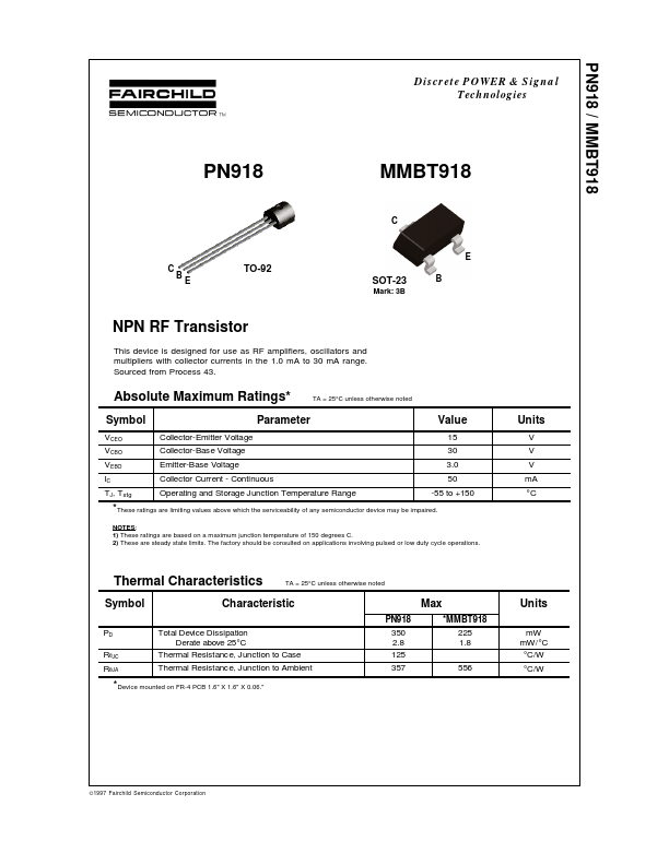
PN918
MMBT918
C
E C B
TO-92
E
SOT-23
Mark: 3B
B
NPN RF Tran...
PN918 / MMBT918
Discrete POWER & Signal Technologies
PN918
MMBT918
C
E C B
TO-92
E
SOT-23
Mark: 3B
B
NPN RF Transistor
This device is designed for use as RF
amplifiers, oscillators and multipliers with collector currents in the 1.0 mA to 30 mA range. Sourced from Process 43.
Absolute Maximum Ratings*
Symbol
VCEO VCBO VEBO IC TJ, Tstg Collector-Emitter
Voltage Collector-Base
Voltage Emitter-Base
Voltage Collector Current - Continuous
TA = 25°C unless otherwise noted
Parameter
Value
15 30 3.0 50 -55 to +150
Units
V V V mA °C
Operating and Storage Junction Temperature Range
*These ratings are limiting values above which the serviceability of any semiconductor device may be impaired.
NOTES: 1) These ratings are based on a maximum junction temperature of 150 degrees C. 2) These are steady state limits. The factory should be consulted on applications involving pulsed or low duty cycle operations.
Thermal Characteristics
Symbol
PD RθJC RθJA
TA = 25°C unless otherwise noted
Characteristic
Total Device Dissipation Derate above 25°C Thermal Resistance, Junction to Case Thermal Resistance, Junction to Ambient PN918 350 2.8 125 357
Max
*MMBT918 225 1.8 556
Units
mW mW/ °C °C/W °C/W
*Device mounted on FR-4 PCB 1.6" X 1.6" X 0.06."
©1997 Fairchild Semiconductor Corporation
PN918 / MMBT918
NPN RF Transistor
(continued)
Electrical Characteristics
Symbol Parameter
TA = 25°C unless otherwise noted
Test Conditions
Min
Max
Units
OFF CHARACTERISTICS
VCEO(sus) V(BR)C...